Multi-layer wiring, method of manufacturing the same and thin film transistor having the same

a thin film transistor and multi-layer technology, applied in the direction of conductors, semiconductor devices, semiconductor/solid-state device details, etc., can solve the problems of affecting the use of aluminum wiring in such display devices, aluminum wiring may also exhibit inferior contact characteristics with other conductive elements of display devices, etc., to achieve the effect of reducing the electrical resistance of wiring, reducing malfunctions such as hillocks or spiking, and reducing the number of defects

Inactive Publication Date: 2007-12-20
LEE JE HUN +3
View PDF0 Cites 2 Cited by
  • Summary
  • Abstract
  • Description
  • Claims
  • Application Information

AI Technical Summary

Benefits of technology

[0009] In one embodiment, the present invention provides a multi-layer wiring exhibiting improved contact characteristics and a reduced tendency to develop malfunctions in the form of hillocks or spiking.
[0013] A multi-layer wiring in accordance with another embodiment of the present invention includes a main wiring and a sub-wiring. The main wiring includes a first metal. The sub-wiring is on a first surface of the main wiring, and includes an alloy to dissipate a thermal stress of the main wiring so as to prevent a deformation of the main wiring and improve contact characteristics. A majority of the alloy is the first metal.
[0014] In another embodiment, the alloy includes the first metal, a second metal for preventing a deformation of the main wiring, and a third metal for improving contact characteristics.
[0017] A TFT in accordance with another embodiment of the present invention includes a gate line, an insulating layer, a channel layer, a data line and a drain electrode. The gate line is on a substrate and is electrically connected to a gate electrode. The gate line includes a main wiring and a sub-wiring. The main wiring includes a first metal. The sub-wiring is on a first surface of the main wiring. The sub-wiring includes an alloy to dissipate a thermal stress of the main wiring so as to prevent a deformation of the main wiring and improve contact characteristics. A majority of the alloy is the first metal. The insulating layer is on the substrate having the gate line and the gate electrode. The channel layer is on a portion of the insulating layer corresponding to the gate electrode. The data line is substantially perpendicular to the gate line on the insulating layer. The data line is electrically connected to a source electrode that is electrically connected to the channel layer. The drain electrode is electrically connected to the channel layer.
[0019] According to various embodiments of the present invention, an electrical resistance of the wiring is decreased, and malfunctions such as hillocks or spiking are decreased. In various embodiments, contact characteristics between the wiring and other conductive elements are additionally improved.

Problems solved by technology

Unfortunately, the use of conventional aluminum wiring in such display devices can be problematic.
Such aluminum wiring may also exhibit inferior contact characteristics with other conductive elements of the display devices.

Method used


Image

  • Multi-layer wiring, method of manufacturing the same and thin film transistor having the same
  • Multi-layer wiring, method of manufacturing the same and thin film transistor having the same
  • Multi-layer wiring, method of manufacturing the same and thin film transistor having the same

Examples


Embodiment Construction

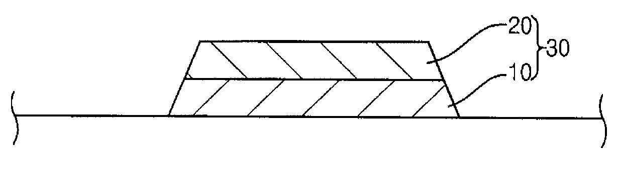
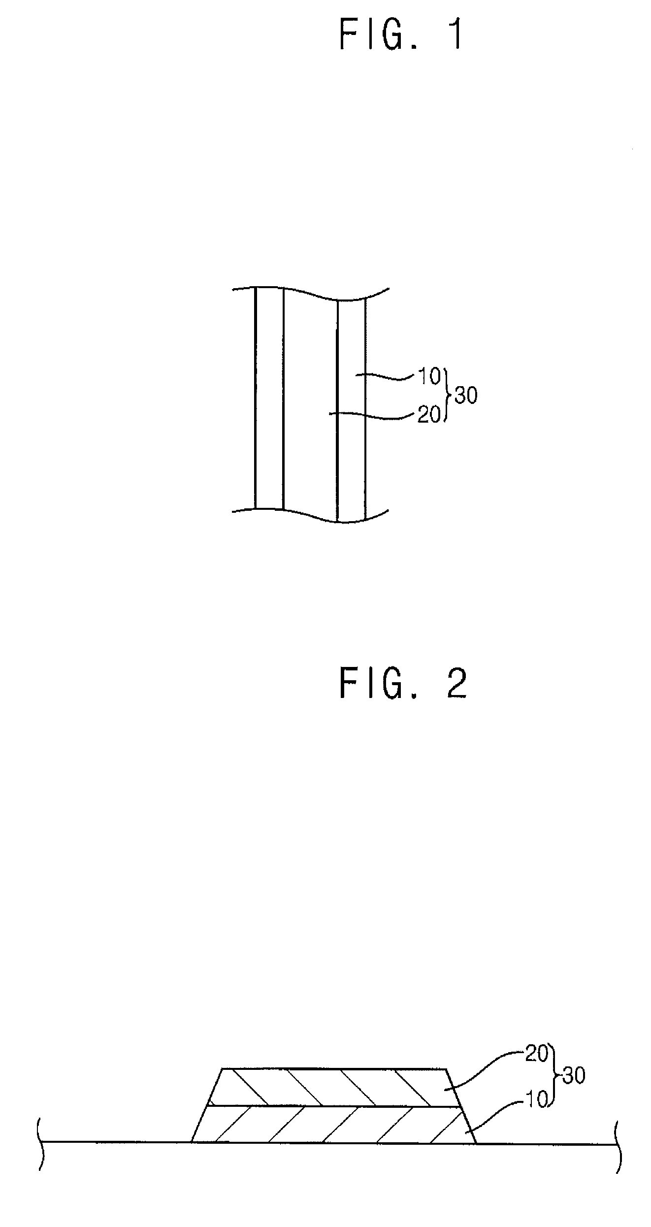
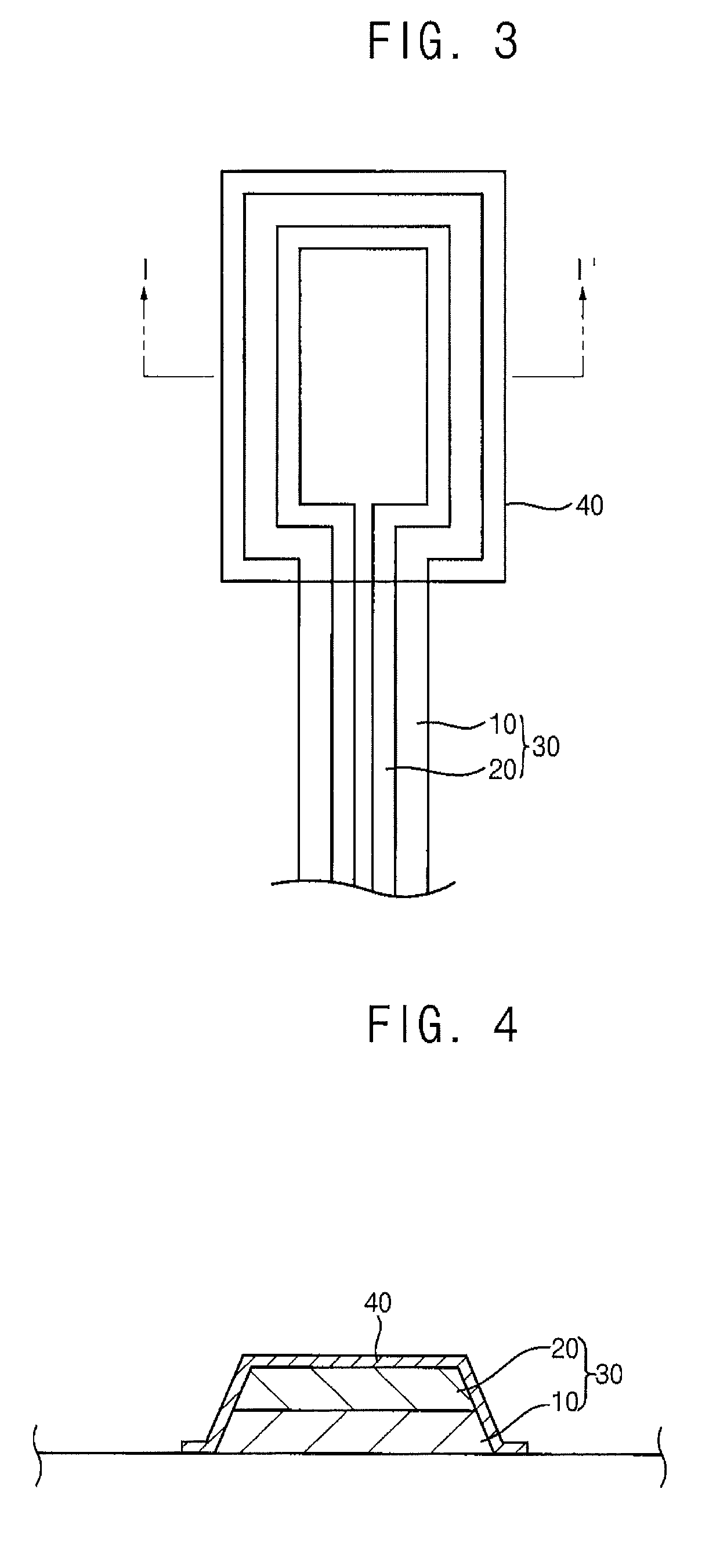
[0039] The invention is described more fully hereinafter with reference to the accompanying drawings, in which embodiments of the invention are shown. The invention may, however, be embodied in many different forms and should not be construed as limited to the embodiments set forth herein. The embodiments are provided for purposes of example only, and not for purposes of limitation. In the drawings, the size and relative sizes of layers and regions may be exaggerated for clarity.

[0040] It will be understood that when an element or layer is referred to as being “on”, “connected to” or “coupled to” another element or layer, it can be directly on, connected, or coupled to the other element or layer, or intervening elements or layers may be present. In contrast, when an element is referred to as being “directly on,”“directly connected to,” or “directly coupled to” another element or layer, there are no intervening elements or layers present. Like numbers refer to like elements througho...


PUM

PropertyMeasurementUnit
temperaturesaaaaaaaaaa
contact resistanceaaaaaaaaaa
thicknessaaaaaaaaaa

Abstract

A multi-layer wiring for use with thin film transistors (TFTs), methods of manufacturing the multi-layer wiring, and TFTs employing the multi-layer wiring are provided. In one embodiment, the multi-layer wiring includes a main wiring and a sub-wiring on the main wiring. The main wiring includes a first metal and the sub-wiring includes an alloy wherein a majority of the alloy is the first metal. The multi-layer wiring can exhibit decreased electrical resistance and a reduced tendency to develop malfunctions such as hillocks or spiking. The multi-layer wiring can also exhibit improved contact characteristics with other conductive elements of TFT display devices.

Description

CROSS-REFERENCE TO RELATED APPLICATIONS [0001] This application is a Continuation Application of co-pending U.S. patent application Ser. No. 11 / 221,492 filed on Sep. 7, 2005, which claims priority to corresponding Korean Patent Application No. 2004-98689 filed in the Korean Intellectual Property Office, Republic of Korea, on Nov. 29, 2004, all of which are hereby incorporated by reference in their entirety.BACKGROUND OF THE INVENTION [0002] 1. Field of the Invention [0003] The present invention relates to wiring for use with thin film transistors (TFTs). More particularly, the present invention relates to a multi-layer wiring for use with TFTs, methods of manufacturing the multi-layer wiring, and TFTs employing the multi-layer wiring. [0004] 2. Description of the Related Art [0005] Flat display devices such as liquid crystal display (LCD) devices, organic light emitting display (OLED) devices, plasma display panel (PDP) devices, and other devices display images based on electric sig...

Claims


Application Information

Patent Timeline
Patent Type & Authority Applications(United States)
IPC IPC(8): H01B5/00
CPCH01L21/76838H01L23/5283H01L23/53209H01L27/12H01L29/4908H01L2924/0002H01L2924/12044H01L2924/00
Inventor LEE, JE-HUNCHO, BEOM-SEOKJEONG, CHANG-OHBAE, YANG-HO
Owner LEE JE HUN
Why Eureka
Try Eureka