Dual panel type organic electroluminescent display device and method for fabricating the same

a display device and electroluminescent technology, applied in the field of dual panel electroluminescent display devices, can solve the problems of deterioration of brightness, limited display size large power consumption of passive matrix organic eld, so as to improve brightness, reduce product cost, and simplify production process

Active Publication Date: 2008-01-17
LG DISPLAY CO LTD
View PDF2 Cites 11 Cited by
  • Summary
  • Abstract
  • Description
  • Claims
  • Application Information

AI Technical Summary

Benefits of technology

[0020]An object of embodiments of the invention is to provide an organic ELD as a top emission type organic ELD to improve brightness.
[0021]Another object of embodiments of the invention is to provide a method of fabricating an organic ELD having a simpler production process to reduce product cost and increase yield.
[0022]Another object of embodiments of the invention is to provide an organic ELD and a method of fabricating the same that can prevent a separation of an emitting layer at a step difference of an array element layer.
[0023]Another object of embodiments of the invention is to provide an organic ELD and a method of fabricating the same that can prevent shorting between a cathode and an anode by degradation of an emitting layer and improve contact characteristics between a driving element and a cathode.

Problems solved by technology

While both the passive matrix organic ELD and the active matrix organic ELD have a simple structure and are formed by a simple fabricating process, the passive matrix organic ELD requires a relatively large amount of power to operate.
In addition, the display size of a passive matrix organic ELD is limited by the width and thickness of conductive lines used in the interconnection of the pixels.
Consequently, because the above-described organic ELD according to the related art is a bottom emission type device, brightness is deteriorated due to the array element reducing the aperture regions of the device.
Further, to prevent minimization of the aperture regions, the design of the array element is limited in a bottom emission type device.
Furthermore, the driving element is typically P-type, which has a complicated fabrication process that reduces product yield.

Method used


Image

  • Dual panel type organic electroluminescent display device and method for fabricating the same
  • Dual panel type organic electroluminescent display device and method for fabricating the same
  • Dual panel type organic electroluminescent display device and method for fabricating the same

Examples


Embodiment Construction

[0049]Reference will now be made in detail to the preferred embodiments, examples of which are illustrated in the accompanying drawings.

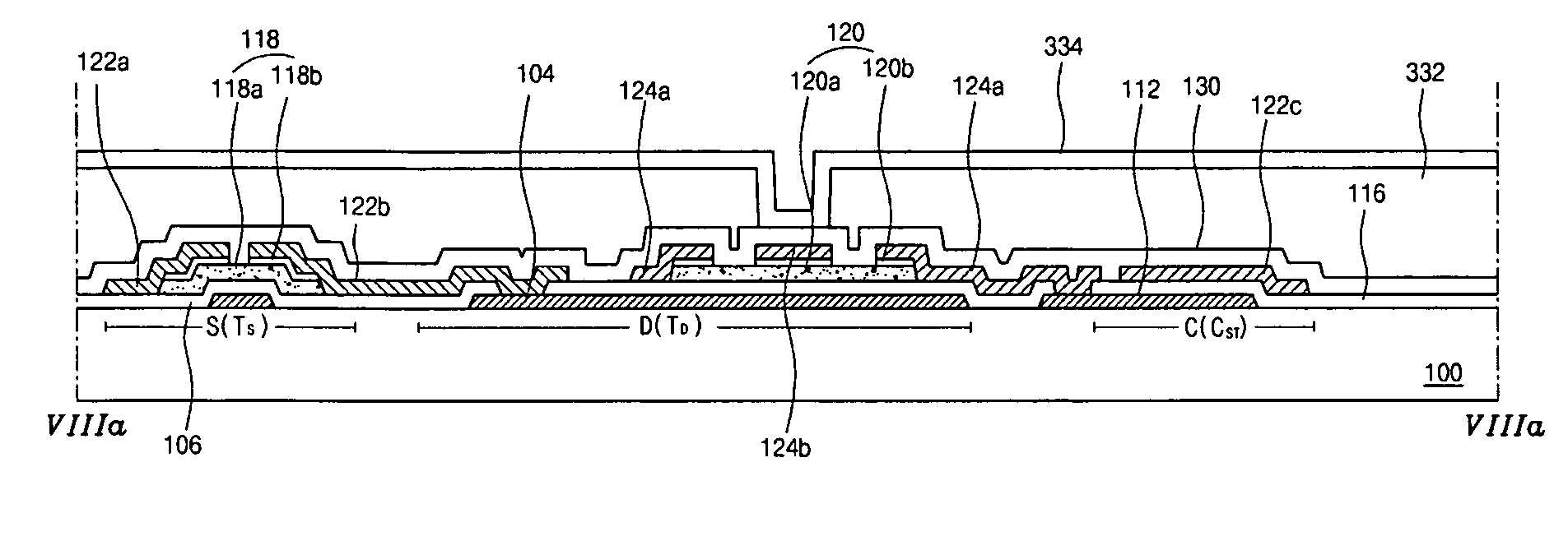
[0050]FIG. 6 is a cross-sectional view of an organic ELD according to an embodiment of the invention. As shown in FIG. 6, an organic ELD “EL” includes a cathode 200 connected to the array element (not shown) on a substrate 100, an electron injection layer 202 on the cathode 200, an electron transport layer 204 on the electron injection layer 202, an emitting layer 206 on the electron transport layer 204, a hole transport layer 208 on the emitting layer 206, a hole injection layer 210 on the hole transport layer 208, and an anode 214 over the hole injection layer 210. The anode 214 can be made of a transparent conductive material, such as indium tin oxide or indium zinc oxide.

[0051]A buffer layer 212 is disposed between the hole injection layer 210 and the anode 214 to prevent damage to the hole injection layer 210 during deposition of the anode 214 ...


PUM


Abstract

An organic electroluminescent device includes a switching element and a driving element connected to the switching element on a substrate in a pixel region, an overcoat layer on the switching element and the driving element, a first contact layer on the overcoat layer, the first contact layer being made of one of molybdenum and indium tin oxide, a cathode on the first contact layer, the cathode connected to the driving element through the first contact layer, an emitting layer on the cathode, and an anode on the emitting layer.

Description

[0001]The present application claims the benefit of Korean Patent Application No. 10-2006-0059352 filed in Korea on Jun. 29, 2006, which is hereby incorporated by reference in its entirety.BACKGROUND OF THE INVENTION[0002]1. Field of the Invention[0003]The embodiments of the invention relates to a display device, and more particularly, to a dual panel type organic electroluminescent display (ELD) device. Although embodiments of the invention are suitable for a wide scope of applications, it is particularly suitable for increasing brightness of an organic electroluminescent display device.[0004]2. Discussion of the Related Art[0005]In general, an organic ELD emits light by injecting electrons from a cathode and holes from an anode into an emission layer such that the electrons combine with the holes to generate an exciton, which then transitions from an excited state to a ground state. In comparison to a liquid crystal display (LCD) device, an additional light source is not necessary...

Claims


Application Information

Patent Timeline
Patent Type & Authority Applications(United States)
IPC IPC(8): H01J1/62
CPCH01L27/3244H01L27/3248H01L2251/5315H01L51/5088H01L51/5221H01L27/3262H10K59/123H10K59/1213H10K59/12H10K50/17H10K50/82H10K2102/3026H05B33/10
Inventor PARK, JAE-HEEPARK, KYUNG-MINLEE, SEOK-JONG
Owner LG DISPLAY CO LTD
Why Eureka
Try Eureka