Method for improving ohmic contact of ZnO film

An ohmic contact, thin film technology, applied in lasers, electrical components, circuits, etc., can solve the problems of complex process and unstable performance of ZnO devices

Inactive Publication Date: 2010-03-31
INST OF SEMICONDUCTORS - CHINESE ACAD OF SCI
View PDF0 Cites 11 Cited by
  • Summary
  • Abstract
  • Description
  • Claims
  • Application Information

AI Technical Summary

Problems solved by technology

[0005] At present, the commonly used methods to improve the ohmic contact of ZnO include rapid thermal annealing, Al doping, etc., but these methods can reduce the contact resistance

Method used


Image

  • Method for improving ohmic contact of ZnO film
  • Method for improving ohmic contact of ZnO film
  • Method for improving ohmic contact of ZnO film

Examples


Embodiment Construction

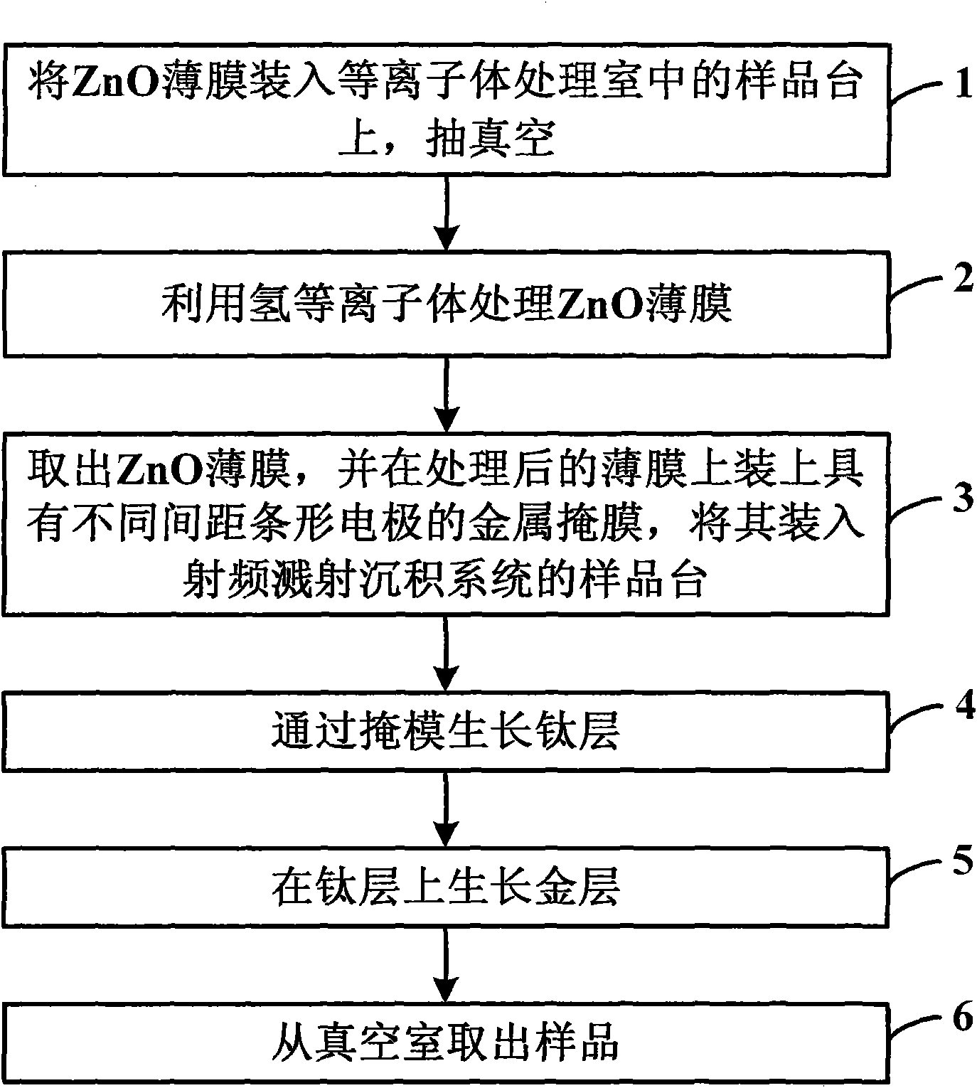
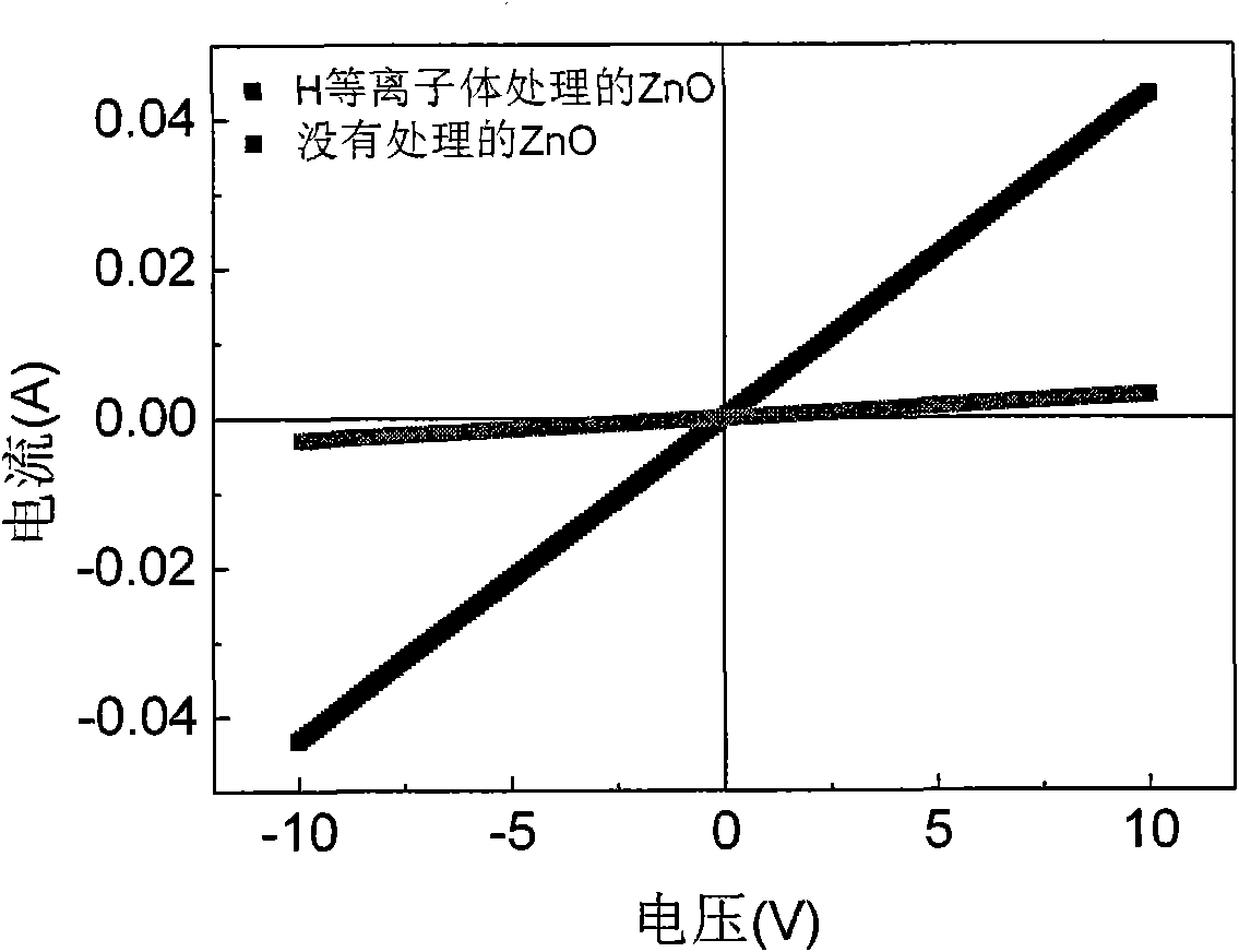
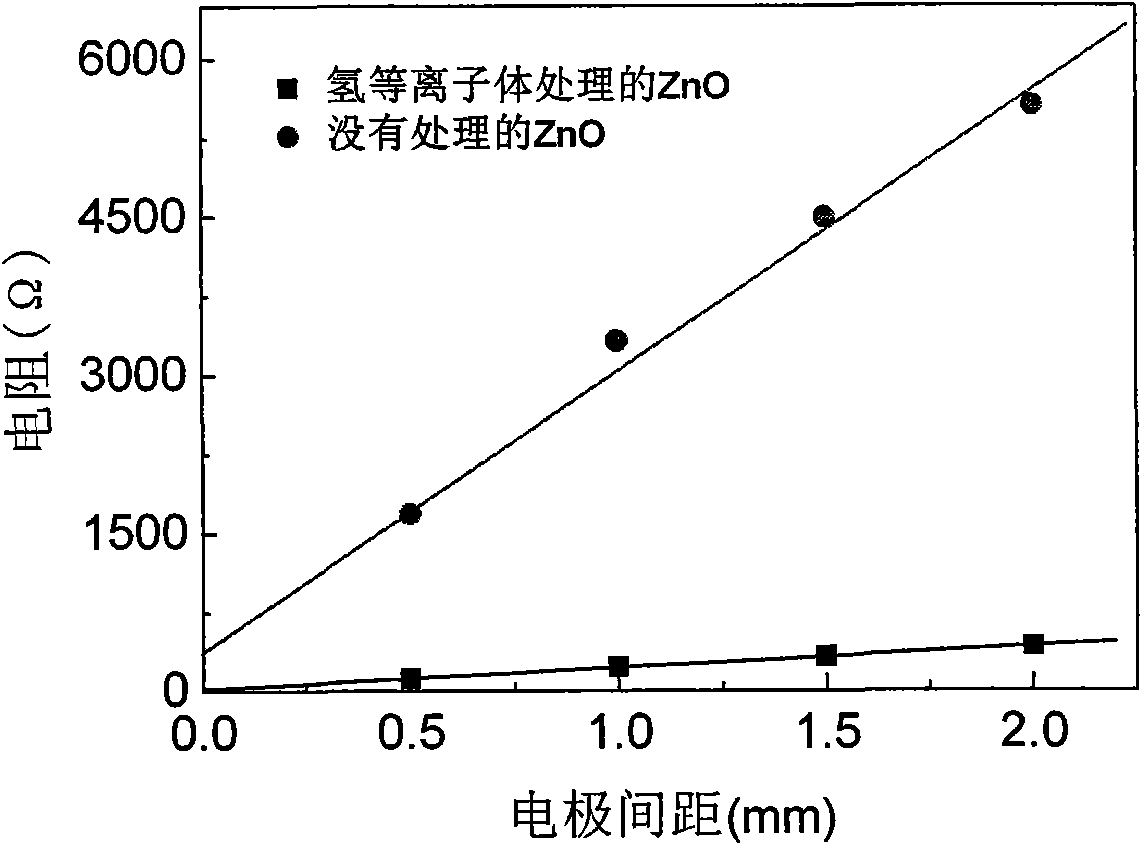
[0023] The first-principle calculations show that the role of hydrogen in ZnO is very different from that of hydrogen in other semiconductors. Hydrogen acts as a recombination center in general semiconductors to neutralize the dominant carriers. However, hydrogen in ZnO It exists as a shallow donor energy level and can have a high concentration. The non-intentionally doped ZnO is n-type. Use hydrogen plasma to treat the ZnO film through a metal mask, so that hydrogen can enter the ZnO film, which can act as a donor in the ZnO film, thereby improving the current-carrying area between the ZnO film and the metal contact area. sub-concentration. Due to the increase of the carrier concentration in the contact area of ​​the ZnO film, the width of the ZnO barrier region becomes very thin, and the electrons pass through the barrier through the tunneling effect to generate a considerable tunneling current, so that its contact resistance can be very small, making the gap between the fil...


PUM


Abstract

The invention discloses a method for improving the ohmic contact of a ZnO film, which comprises the following steps of: utilizing a hydrogen plasma to treat an electrode contact area of the ZnO film before a metal electrode is deposited; and then depositing a double-layer metal electrode in the electrode contact area of the ZnO film treated by the hydrogen plasma to form the ohmic contact. The treatment of the hydrogen plasma causes hydrogen to be diffused into the ZnO film, which improves the carrier concentration of the ZnO film in the contact area, and reduces the resistivity of the ZnO film in the contact area so as to remarkably reduce the contact resistance of the ZnO film and metal and improve the ohmic contact characteristics thereof. In addition, in MS technology, sputtered particles have higher energy, so ZnO/Ti interfacial atoms can be fully mixed, and the adhesion of the Ti/Au contact on the ZnO film can be improved. The ohmic contact with good adhesion and low contact resistance can be obtained by the method, and a foundation is laid for realizing ZnO film electronic devices.

Description

technical field [0001] The invention relates to the technical field of semiconductors, in particular to a method for improving the ohmic contact of a ZnO thin film. Background technique [0002] ZnO is an important II-VI wide bandgap and direct bandgap semiconductor material. At room temperature, its bandgap width is 3.37eV, and the exciton binding energy is 60meV. It is considered to be another new type after ZnSe and GaN. Optoelectronic materials are the best candidate materials for short-wavelength light-emitting diodes (LEDs) and semiconductor lasers. They have a wide range of uses in high-tech fields such as information storage and display, optical communications, semiconductor white light lighting, medicine, and biology. They are the current semiconductor material science and device research hotspots. [0003] At present, people have been able to use methods such as molecular beam epitaxy (MBE), metal organic chemical vapor deposition (MOCVD) and magnetron sputtering ...

Claims


Application Information

Patent Timeline
IPC IPC(8): H01L21/28H01L21/285H01L21/461H01L33/00H01S5/00
Inventor 张兴旺蔡培锋游经碧范亚明高云陈诺夫
Owner INST OF SEMICONDUCTORS - CHINESE ACAD OF SCI
Why Eureka
Try Eureka