Light emitting diode structure

a technology of light-emitting diodes and diodes, which is applied in the direction of basic electric elements, electrical apparatus, and semiconductor devices, can solve the problems of reducing the luminous efficiency of the diodes, reducing the manufacture cost of the diodes, and restricting the emitting area of the diodes, so as to achieve high conductivity and facilitate the generation of contact layers

Inactive Publication Date: 2007-12-20
EPILEDS TECH
View PDF1 Cites 11 Cited by
  • Summary
  • Abstract
  • Description
  • Claims
  • Application Information

AI Technical Summary

Benefits of technology

[0007]Thus, one purpose of the present invention is to provide an LED structure to form a contact layer of ...

Problems solved by technology

Consequently, the light emitting area of the diode is restrained, and it is unable to take full advantage of the active layer, thereby reducing the luminous efficiency of the diode substantially.
As a whole, the high concentration P-type doped layer cannot grow efficiently since the conventional diode structure is limited due to the physical characteristics of the contact layer, ...

Method used


Image

  • Light emitting diode structure
  • Light emitting diode structure
  • Light emitting diode structure

Examples


Embodiment Construction

[0018]The features and the advantages of the present invention will be readily understood upon a thoughtful deliberation of the following detailed description of a preferred embodiment of the present invention with reference to the accompanying drawings.

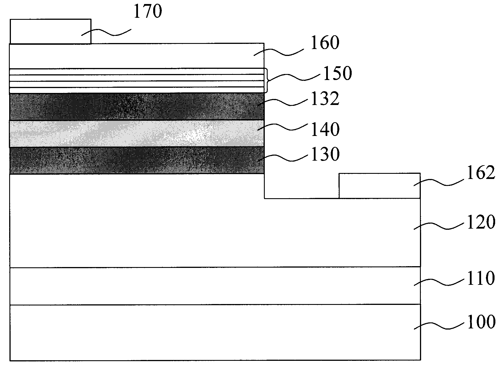
[0019]Since a multilayer structure grows easily into a diode's contact layer made of nitride semiconductor material of high conductivity (high carrier concentration), the current may not be limited to the electrode thanks to lower resistance characteristics and better current spreading. And, the contact layer made of the multilayer structure has a higher carrier concentration than the bulk layer, so the subsequent transparent electrode can easily generate Ohmic contact with it, rather than Schottky contact that leads to higher operating voltage of elements due to insufficient carrier concentration. In addition, the transparent electrode and the contact layer of multilayer structure can be made of the same conducting materials so that...


PUM


Abstract

A LED (Light Emitting Diode) structure with a contact layer of a multiple structure includes a nucleation layer disposed on a substrate; a conductive buffer layer disposed on the nucleation layer; an active layer disposed between an upper and a lower confinement layer, wherein the structure of active layer includes a semiconductor material mainly doped with III-V group; the contact layer made of the multilayer structure disposed on the upper confinement layer; and a transparent electrode disposed on the contact layer made of a multilayer structure; and an electrode contacted with the conductive buffer layer and isolated from the active layer and the transparent electrode.

Description

BACKGROUND OF INVENTION[0001]1. Field of the Invention[0002]The present invention generally relates to a light emitting diode (LED), and more particularly to a LED structure which has a contact layer made of a multilayer structure.[0003]2. Description of Related Art[0004]LED elements made of compound semiconductor materials have recently attracted the attention of many people. FIG. 1 depicts a sectional view of a LED doped with commonly used III-V group elements. As shown in FIG. 1, the LED is formed on a substrate 10 such as Al2O3 (aluminum oxide) substrate. A nucleation layer 12 and an N-type conductive buffer layer 14 are on the substrate 10 in order. The buffer layer 14 doped with N-type GaN (gallium nitride) is used for smoother subsequent crystal growing. An active layer 18 for light emitting is on the buffer layer 14, where an upper and lower confinement layer or cladding layers 16, 20 are formed. The lower confinement layer 16 is doped with N-type GaN when the upper confinem...

Claims


Application Information

Patent Timeline
IPC IPC(8): H01L33/00H01L31/12H01L27/15H01L29/26H01L33/12H01L33/14H01L33/32
CPCH01L33/12H01L33/32H01L33/14
Inventor KU, CHIN-FUHSU, MING-SEN
Owner EPILEDS TECH
Why Eureka
Try Eureka