Printed circuit board and circuit structure for power supply
- Summary
- Abstract
- Description
- Claims
- Application Information
AI Technical Summary
Benefits of technology
Problems solved by technology
Method used
Image
Examples
embodiment 1
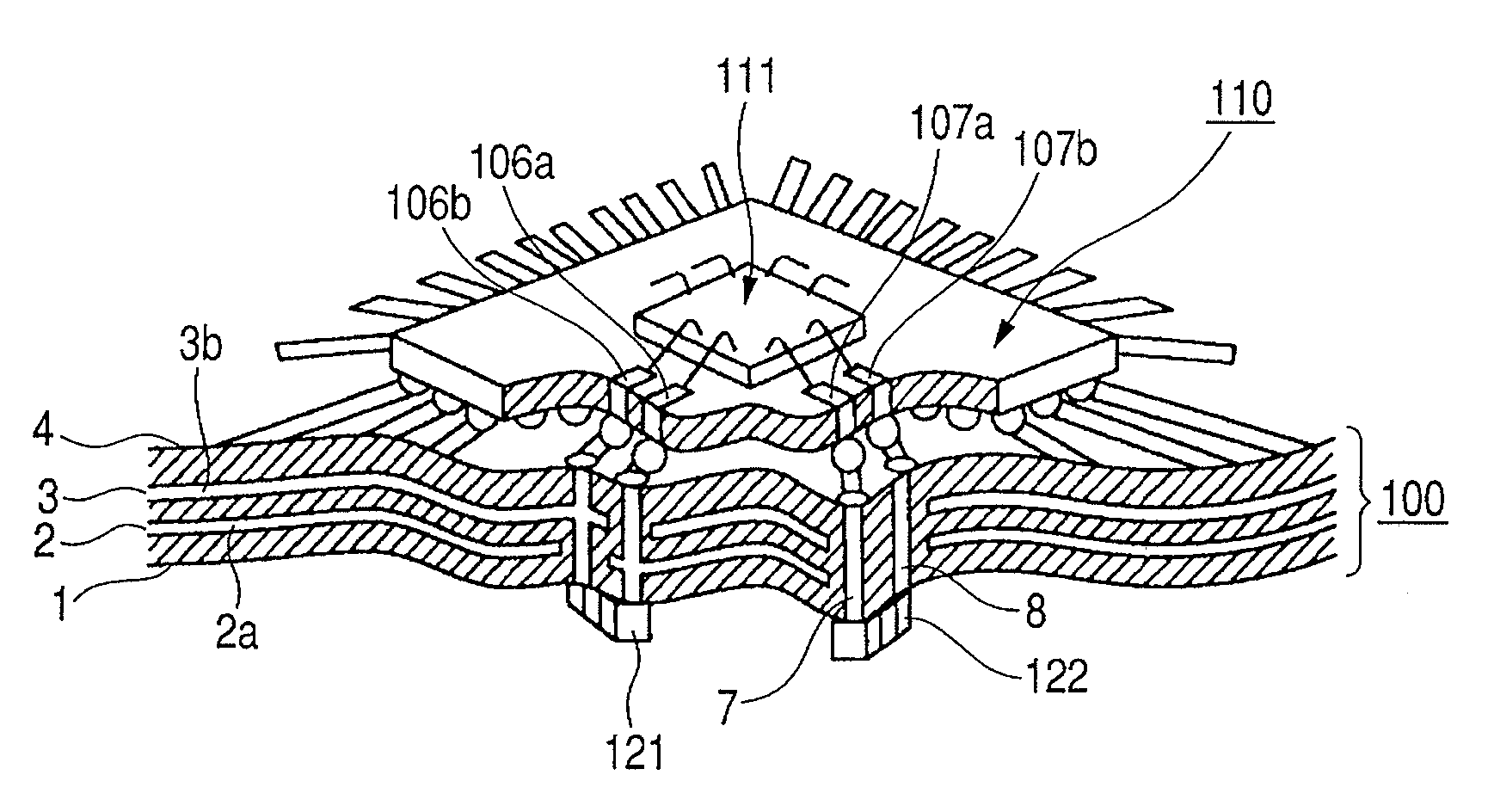
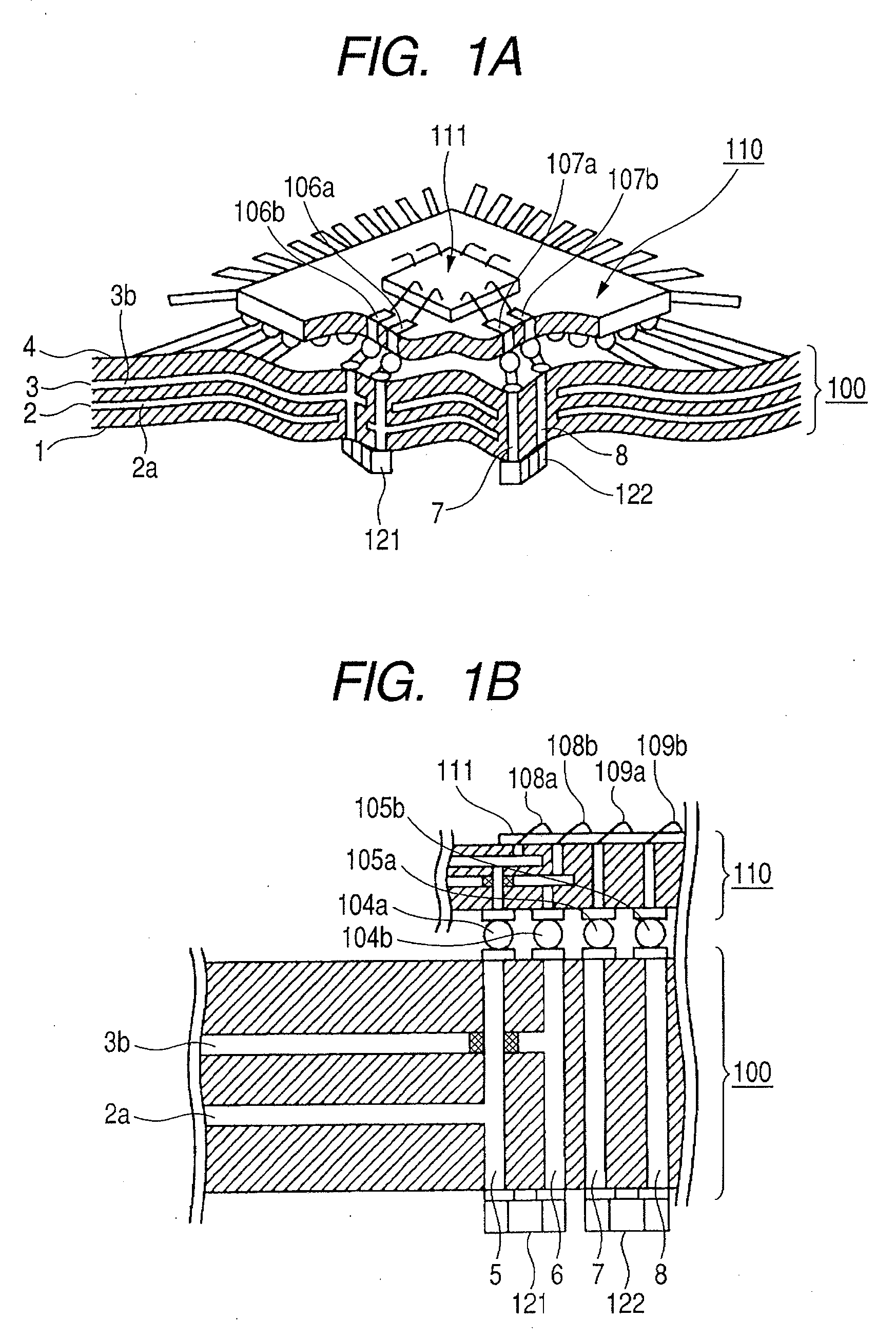
[0068]FIGS. 1A and 1B illustrate a printed circuit board according to Embodiment 1 of the present invention. FIG. 1A is a perspective view illustrating the printed circuit board which is partially cut away to facilitate the understanding of the present invention. FIG. 1B is a cross sectional view illustrating the printed circuit board of FIG. 1A.
[0069]A printed wiring board 100 includes circuits formed therein. An IC package 110 having a BGA structure is mounted on the printed wiring board 100. The IC package 110 is provided with an IC chip 111. Although the IC chip 111 located on the IC package 110 is normally molded with a resin, the resin is omitted here.
[0070]The printed wiring board 100 has a four-layer structure and includes a back surface signal wiring layer 1, a power supply layer 2, a ground (GND) layer 3, and a front surface signal wiring 4. The power supply layer 2 and the GND layer 3 are connected to a source power supply 101 (not shown here). A power supply terminal 104...
example 1
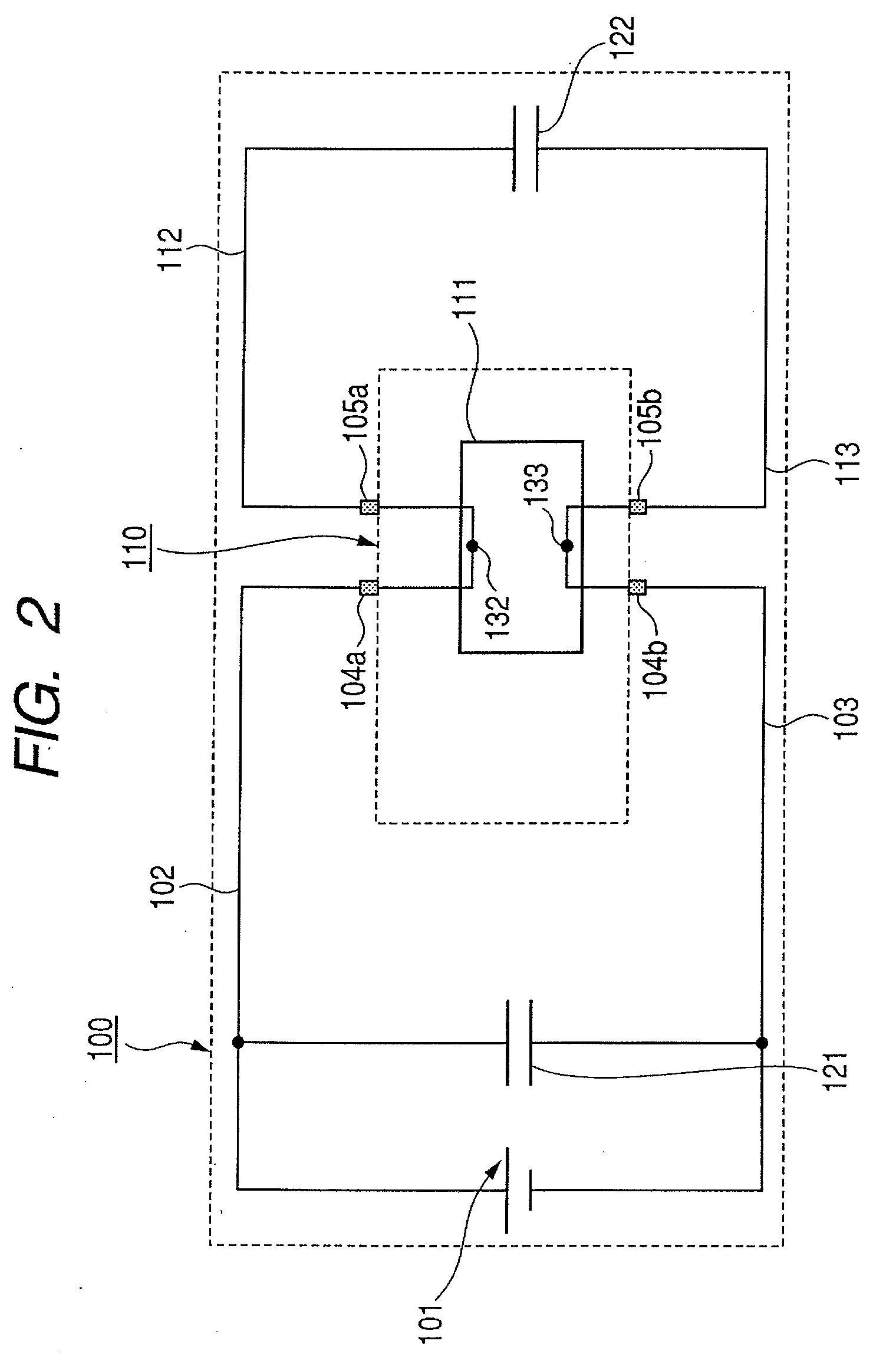
[0079]In order to examine an effect of the circuit structure illustrated in FIG. 2, a simulation is performed. FIG. 3 is a circuit diagram illustrating a circuit structure for simulation. The first circuit located on the power supply side of the IC chip 111 is modeled using the source power supply 101, supply-side power supply paths 102a, 102b, and 102c, supply-side GND paths 103a, 103b, and 103c, and the bypass capacitor 121.
[0080]The source power supply 101 is a source power supply. Reference numeral 111 denotes an IC chip. The purpose of this simulation is to evaluate the characteristic of the power supply path between the source power supply 101 and the IC chip 111, so the source power supply and the IC chip are assumed as an input or output of the power supply path and thus not modeled. It is assumed that the power supply path 102a is a line whose width is 50 mm and length is 50 mm, L=4.9e-09 H / cm, C=9.5454e-09 F / cm, R(DC)=0.011 Ω / cm, Rs=4.01609262841384e-06 (Ω·ns) 0.5 / cm, and ...
example 2
[0097]Next, Example 2 of the present invention will be described. The bypass capacitor 122 provided in Example 1 is used to reduce the noise in the vicinity of 100 MHz and has a capacitance of 1000 pF. In Example 2, assuming that the frequency for reduction is in the vicinity of the 300 MHz, the capacitance of the bypass capacitor 122 is changed from 1000 pF to 200 pF. As in the case of Example 1, a simulation was performed using the circuit structure illustrated in FIG. 3, except for the fact that the capacitance of the bypass capacitor 122 is changed to 200 pF.
[0098]FIG. 22A illustrates a Z11 characteristic as observed from the IC chip 111 at respective frequencies. In FIG. 22A, the resonance point of a low impedance sin the vicinity of 10 MHz may be caused by the bypass capacitor 121 and the resonance point of a low impedance in the vicinity of 300 MHz may be caused by the bypass capacitor 122. The resonance point at higher frequencies may be caused by the characteristic of the e...
PUM
 Abstract
Description
Claims
Application Information


