Methods of fabricating active device array substrate and fabricating color filter substrate

Active Publication Date: 2007-12-20
AU OPTRONICS CORP
View PDF7 Cites 4 Cited by
  • Summary
  • Abstract
  • Description
  • Claims
  • Application Information

AI Technical Summary

Benefits of technology

[0009]In view of the above, an objective of the present invention is to provide a method of fabricating an active device array substrate, which can eliminate the mura of MVA LCD, and improve the transmittance and aperture ratio.
[0010]Another objective of the present invention is to provide a method of fabricating a color filter substrate, which can eliminate the mura of MVA LCD, and improve the transmittance and aperture ratio.
[0031]In the methods for fabricating an active device array substrate and fabricating a color filter substrate of the present invention, the alignment method of alignment films employs the inkjet printing process to form mask layers in specific regions. Compared with the conventional art using the lithography process to form mask layers, the methods of fabricating an active device array substrate and fabricating a color filter substrate of the present invention have the advantages of being simple and low cost. The fabricated active device array substrate and color filter substrate can be used to assemble an LCD panel, so as to make the liquid crystal molecules being arranged in different directions. Therefore, the present invention can achieve the LCD panel with wide viewing angle without using the designs of slit patterns or protrusions. In addition, the LCD panel assembled by the active device array substrate and / or color filter substrate of the present invention has higher aperture ratio and transmittance, and mura does not easily occur.

Problems solved by technology

However, the ion beam alignment method must employ a lithography process to form the mask, and due to the mask and exposure process, the process is complicated and has a high cost.
However, electric field near the protrusions or slit patterns is non-uniform, thus easily resulting in the defect of mura.
Moreover, the design of protrusions and slit patterns also reduces the transmittance and aperture ratio of the display panel.

Method used


Image

  • Methods of fabricating active device array substrate and fabricating color filter substrate
  • Methods of fabricating active device array substrate and fabricating color filter substrate
  • Methods of fabricating active device array substrate and fabricating color filter substrate

Examples


Embodiment Construction

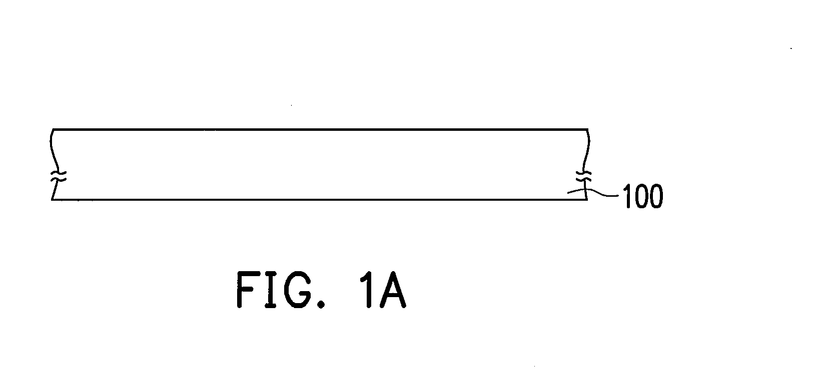
[0036]FIG. 1A to FIG. 10 are flow charts of the method of fabricating an active device array substrate according to an embodiment of the present invention. In order to clearly illustrate the processes of the method of fabricating an active device array substrate, the top view and sectional view are simultaneously shown in some figures. Referring to FIG. 1A, the method of fabricating an active device array substrate comprises providing a substrate 100, and the substrate 100 is, for example, a glass substrate, a quartz substrate, or a substrate made of another appropriate material.

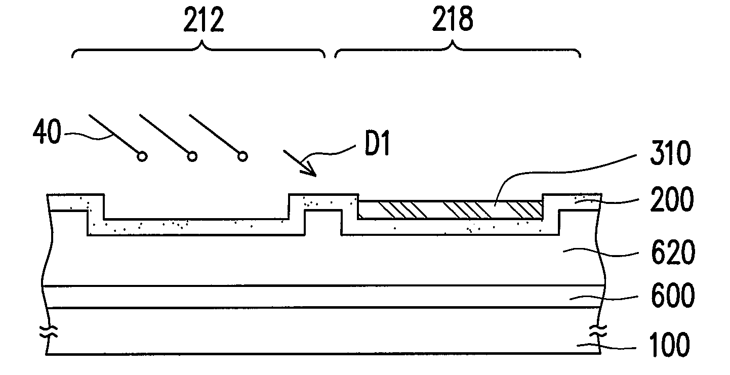
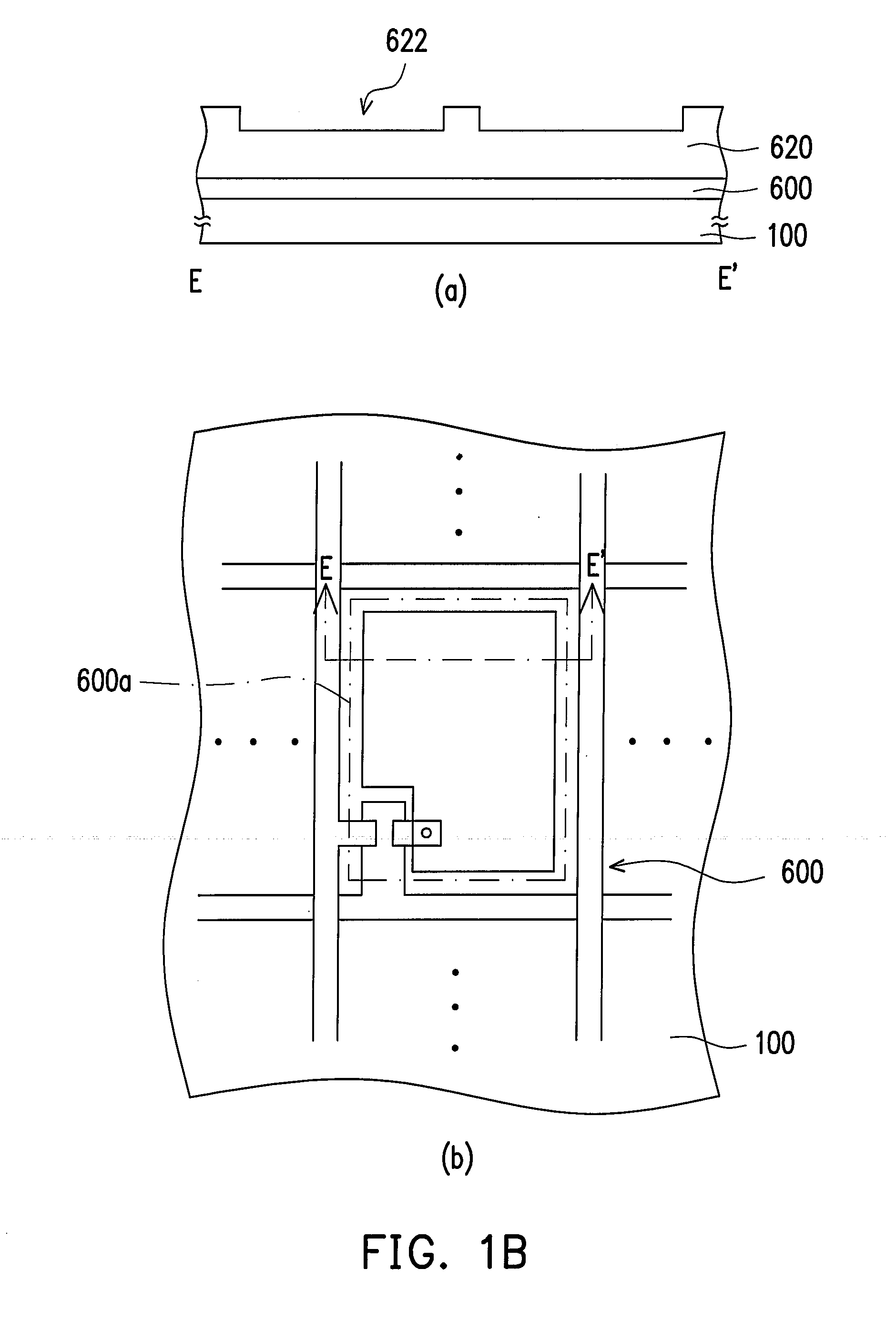
[0037]Referring to FIG. 1B, a pixel array 600 having a plurality of sub-pixels 600a is formed on the substrate 100. After forming the pixel array 600, an insulating layer 620 is further formed on the pixel array 600. In a preferred embodiment, the insulating layer 620 has a plurality of recesses 622.

[0038]Referring to FIG. 1C, an alignment material layer 200 is formed on the pixel array 600, and the material...


PUM


Abstract

A method of fabricating an active device array substrate is provided. First, a substrate is provided. A pixel array is formed on the substrate. An alignment material layer having a plurality of alignment regions is formed on the pixel array. A mask layer is formed on a portion of the alignment regions on the alignment material layer by using an inkjet printing process, so as to expose another portion of the alignment regions on the alignment material layer. Then, a particle beam alignment process is performed to the exposed alignment material layer. Then, the mask layer is removed. Another mask layer is formed on the alignment material layer which has been treated by the particle beam to expose the alignment material layer not treated by the particle beam. Another particle beam alignment process is performed to the exposed alignment material layer, and then the another mask layer is removed.

Description

CROSS-REFERENCE TO RELATED APPLICATION[0001]This application claims the priority benefit of Taiwan application serial no. 95122006, filed on Jun. 20, 2006. All disclosure of the Taiwan application is incorporated herein by reference.BACKGROUND OF THE INVENTION[0002]1. Field of Invention[0003]The present invention relates to methods of fabricating an array substrate and fabricating a filter substrate. More particularly, the present invention relates to methods of fabricating an active device array substrate and fabricating a color filter substrate of a liquid crystal display (LCD).[0004]2. Description of Related Art[0005]In current society, multimedia technology has been well developed, which mostly benefits from the development of semiconductor devices or display apparatuses. Among displays, liquid crystal displays, due to the superior characteristics of high picture quality, good space utilization, low power consumption, and radiation free, has gradually become the mainstream produ...

Claims


Application Information

Patent Timeline
IPC IPC(8): G02F1/1337G02F1/1335H01L21/00
CPCG02F1/133788G02F1/133753
Inventor TUNG, YUAN-HUNGTING, CHIN-KUO
Owner AU OPTRONICS CORP
Why Eureka
Try Eureka