High-frequency module

a high-frequency module and module technology, applied in the field of high-frequency modules, can solve the problems of noise induced, crosstalk between the antenna terminals, and the separation characteristics between the two antenna terminals deteriorating, and achieve excellent separation characteristics

Active Publication Date: 2007-12-27
MURATA MFG CO LTD
View PDF2 Cites 27 Cited by
  • Summary
  • Abstract
  • Description
  • Claims
  • Application Information

AI Technical Summary

Benefits of technology

[0010] In order to overcome the problems described above, preferred embodiments of the present invention provide a high-frequency module including a plurality of antenna terminals and having excellent separation characteristics.

Problems solved by technology

In such an antenna duplexer, the physical distance between the two antenna terminals corresponding to different frequency bands is small, and therefore, the separation characteristics (isolation characteristics) between the two antenna terminals deteriorates.
That is, crosstalk occurs between the antenna terminals and noise is induced.
Thus, crosstalk between the wirings in the module substrate easily occurs.
At that time, the physical distance between wirings formed on the surface of the module mounting substrate becomes small, and therefore, the separation characteristics deteriorate.

Method used


Image

  • High-frequency module
  • High-frequency module
  • High-frequency module

Examples


first preferred embodiment

[0038] A high-frequency module according to a first preferred embodiment of the present invention is described below with reference to FIGS. 1 to 14.

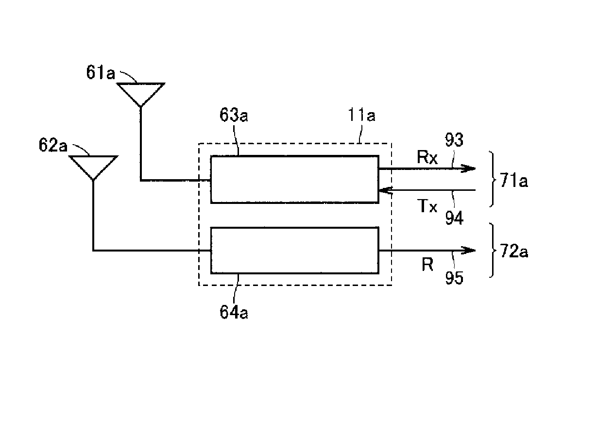
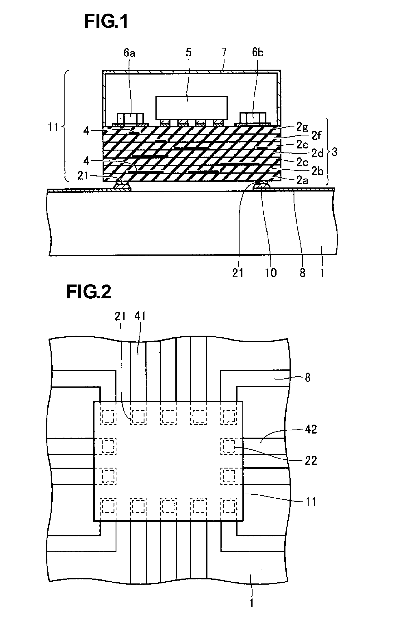
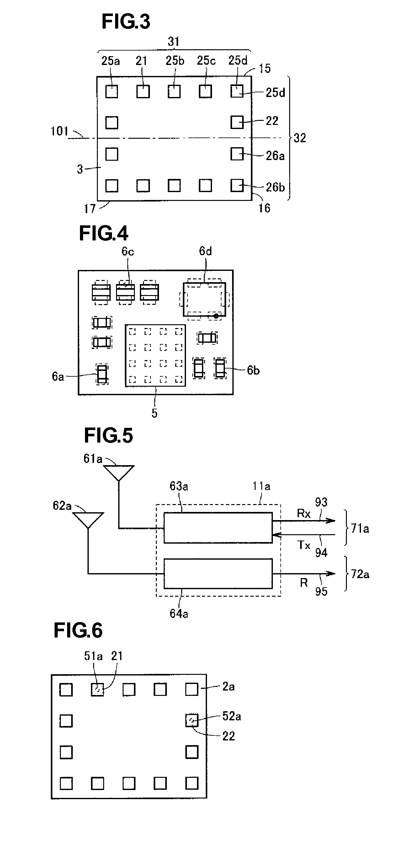
[0039]FIG. 1 is a schematic illustration of a cross sectional view of the high-frequency module according to the present preferred embodiment when mounted on a module mounting substrate. FIG. 2 is a schematic illustration showing a plan view of the high-frequency module when mounted on the module mounting substrate. As shown in FIGS. 1 and 2, a plurality of terminals disposed on a first surface of a high-frequency module 11 are electrically connected to the upper surface of an wiring electrode 8 disposed on a surface of a printed circuit board 1 defining a module mounting substrate via a connecting material, such as a solder 10, for example. Thus, the high-frequency module 11 is provided.

[0040] The high-frequency module 11 includes a multilayer substrate 3 defining a body. The multilayer substrate 3 includes stacked dielectric layers ...

second preferred embodiment

[0075] A high-frequency module according to a second preferred embodiment of the present invention is described below with reference to FIGS. 15 and 16.

[0076]FIG. 15 is a plan view of the high-frequency module according to the present preferred embodiment when an upper cover thereof is removed. FIG. 16 is a bottom view of the high-frequency module according to the present preferred embodiment. According to the present preferred embodiment, the high-frequency module includes a multilayer substrate 81. Two IC chips 82a and 82b and external elements 83a to 83c (such as a stacked capacitor or a stacked inductor) are disposed on the surface of the multilayer substrate 81 remote from a module mounting substrate that is connected to the multilayer substrate 81.

[0077] A plurality of terminals 86 are disposed on the bottom surface of the multilayer substrate 81. The plurality of terminals 86 include a first antenna terminal 84 and a second antenna terminal 85. The multilayer substrate 81 p...

third preferred embodiment

[0080] A high-frequency module according to a third preferred embodiment of the present invention is described below with reference to FIGS. 17 and 18.

[0081]FIG. 17 is a schematic illustration showing a cross-sectional view of the high-frequency module according to the present preferred embodiment. FIG. 18 is a bottom view of the high-frequency module according to the present preferred embodiment.

[0082] According to the present preferred embodiment, the high-frequency module includes a multilayer substrate 87 and external elements 82a, 83a, and 83b disposed on a surface of the multilayer substrate 87. The external element 82a is an active component (such as an IC chip). The external elements 83a and 83b are passive components (such as stacked capacitors). Additionally, the high-frequency module according to this preferred embodiment includes an outer case 91 that is arranged so as to cover the external elements 82a, 83a, and 83b.

[0083] According to the present preferred embodimen...


PUM


Abstract

A high-frequency module is integrally formed from at least some circuit components defining a first wireless system using a first frequency band and at least some circuit components defining a second wireless system using a second frequency band. The high-frequency module includes a multilayer substrate including a plurality of stacked dielectric layers, a first terminal group disposed on a first surface of the multilayer substrate, where a plurality of terminals are arranged along a first side of four sides defining the first surface, and a second terminal group disposed on the first surface, where a plurality of terminals are arranged along a second side that is different from the first side. The first terminal group includes a first antenna terminal of the first wireless system whereas the second terminal group includes a second antenna terminal of the second wireless system.

Description

BACKGROUND OF THE INVENTION [0001] 1. Field of the Invention [0002] The present invention relates to a high-frequency module and, in particular, to a high-frequency module including a multilayer substrate having a resistor and a coil disposed therein. [0003] 2. Description of the Related Art [0004] In recent years, wireless apparatuses, such as cell phones and wireless LANs (Local Area Networks) have become highly functional and the sizes of the wireless apparatuses have been decreased. Among such highly functional apparatuses, a wireless apparatus that can handle signals in a plurality of frequency bands has been developed. In order to decrease the size of the wireless apparatus that can handle signals in a plurality of frequency bands, a wireless module has been developed into which some of the parts of a wireless system, in particular, front-end parts are integrated as one package. [0005] For example, Japanese Unexamined Patent Application Publication No. 2000-349586 describes an...

Claims


Application Information

Patent Timeline
Patent Type & Authority Applications(United States)
IPC IPC(8): H03H7/46H04B1/38H04B1/3822H05K3/46
CPCH01L2223/6688H01L2224/16225H01L2924/09701H01L2924/15153H01L2924/15165H01L2924/15311H01L2924/1532H01L2924/16152H01L2924/19105H01L2924/19106H01L2924/3025H04B1/005H04B1/0067H05K1/0298H05K1/141H05K1/16H05K1/183H05K3/3442H01L23/48H01L23/66H01L2223/6677H01L2924/01004H01L2224/04042H01L25/04H01L25/18H05K3/46
Inventor HOSOKAWA, TOSHIHIROHIGASHIBATA, KAZUAKISUESADA, TSUYOSHI
Owner MURATA MFG CO LTD
Why Eureka
Try Eureka