Rectangular Semi-Conducting Support for Microelectronics and Method for Making Same

a semi-conducting support and microelectronic technology, applied in the direction of solid-state devices, electric devices, basic electric elements, etc., can solve the problems of limiting production rate, large cost, and replacing processing machines

Active Publication Date: 2008-01-03
COMMISSARIAT A LENERGIE ATOMIQUE ET AUX ENERGIES ALTERNATIVES
View PDF6 Cites 12 Cited by
  • Summary
  • Abstract
  • Description
  • Claims
  • Application Information

AI Technical Summary

Problems solved by technology

Thus, when the diameter of the supports is increased with the aim of increasing productivity, the processing machines have to be replaced, which represents large costs.
In addition, the circular shape of the semi-conducting supports makes processing of the supports difficult and therefore limits the production rate.
With these supports, it is difficult to achieve double-sided components, i.e. components comprising electronic elements on both surfaces, in particular their front and rear surfaces.
The main problem is the mechanical strength of silicon.
A silicon support is in fact liable to break when electronic elements are realized on both its surfaces.
Furthermore, the amount of heat generated by integrated circuits increases with the power of the circuits which is increasing all the time.
Heat dissipation is therefore becoming an increasingly important problem.

Method used


Image

  • Rectangular Semi-Conducting Support for Microelectronics and Method for Making Same
  • Rectangular Semi-Conducting Support for Microelectronics and Method for Making Same
  • Rectangular Semi-Conducting Support for Microelectronics and Method for Making Same

Examples


Embodiment Construction

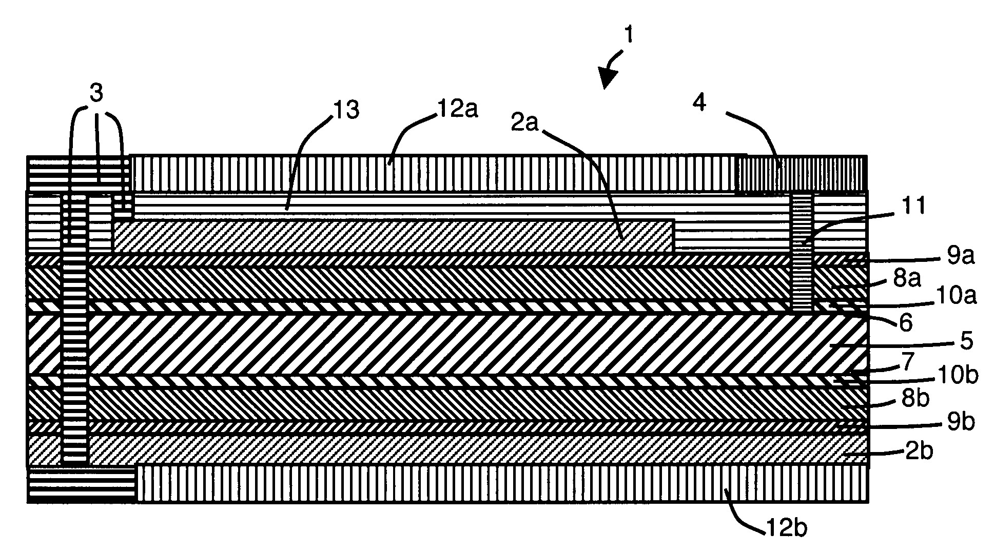
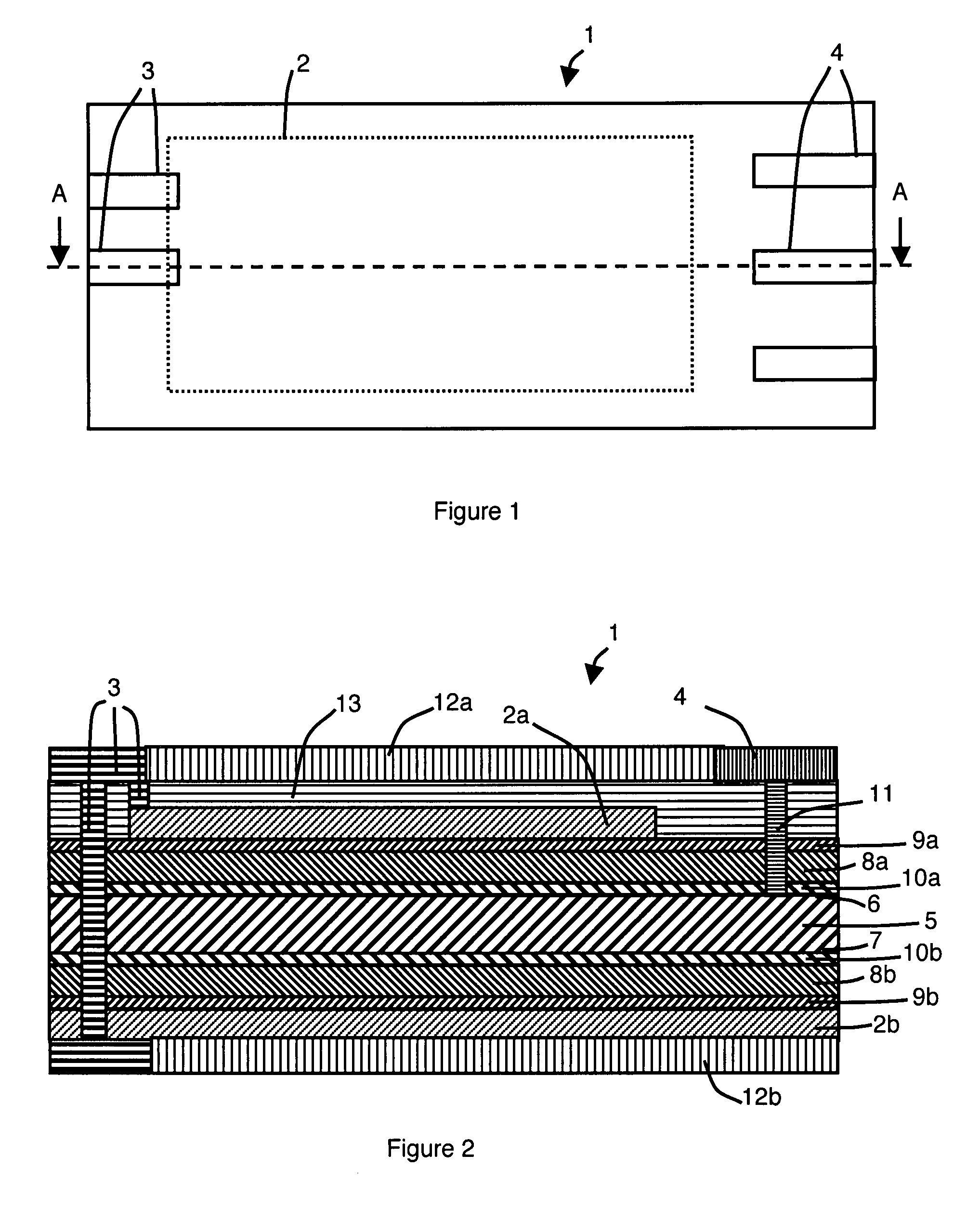
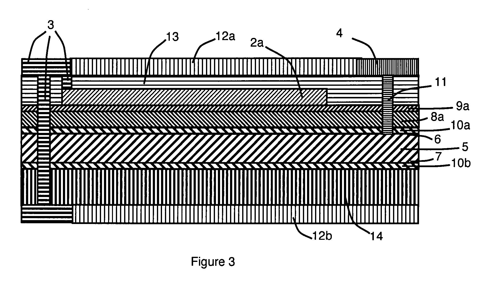
[0011]FIG. 1 illustrates a front surface of a rectangular semi-conducting support 1 comprising at least one integrated circuit in a semi-conducting layer 2. The integrated circuit can be electrically connected to the rear surface of the support 1 by means of electrical connections 3 passing through the support 1. In addition, the support 1 can comprise heat sinks 4 arranged on an external surface of the support 1, for example on the front surface as represented, and connected to internal layers of the support 1 by means of a thermal connection, enabling the internal layers to be cooled when the integrated circuit is operating. The thermal connections can be connected to external cold sources. The support can also comprise electrical connection pads to connect the integrated circuit to external devices.

[0012] The support 1 represented in FIG. 2 comprises a graphite substrate 5 having a front surface 6 and a rear surface 7, respectively arranged at the top and bottom in FIG. 2. The s...


PUM

PropertyMeasurementUnit
widthaaaaaaaaaa
widthaaaaaaaaaa
dielectric constantaaaaaaaaaa

Abstract

The semi-conducting support comprises a graphite substrate having a front surface and a rear surface and at least a first stack arranged on the front surface of the substrate. The first stack successively comprises a single-crystal diamond layer, an electrically insulating oxide layer and a semi-conducting layer. The support can comprise a second stack arranged on the rear surface of the substrate and comprising the same succession of layers as the first stack or comprising a polymer material layer. A thermal connection passing through the first and / or second stacks and connecting the graphite substrate to an external surface of the support enables heat to be removed. The method can comprise production of the semi-conducting layer by molecular bonding of rectangular silicon strips onto the oxide layer.

Description

BACKGROUND OF THE INVENTION [0001] The invention relates to a semi-conducting support for microelectronics. STATE OF THE ART [0002] Generally, semi-conducting supports used for microelectronics are circular and the support processing machines are adapted to the diameter of the supports. Thus, when the diameter of the supports is increased with the aim of increasing productivity, the processing machines have to be replaced, which represents large costs. In addition, the circular shape of the semi-conducting supports makes processing of the supports difficult and therefore limits the production rate. [0003] Semi-conducting supports are in most cases silicon supports. With these supports, it is difficult to achieve double-sided components, i.e. components comprising electronic elements on both surfaces, in particular their front and rear surfaces. The main problem is the mechanical strength of silicon. A silicon support is in fact liable to break when electronic elements are realized o...

Claims


Application Information

Patent Timeline
Patent Type & Authority Applications(United States)
IPC IPC(8): H01L23/06H01L21/31
CPCH01L23/3732H01L2924/0002H01L2924/00
Inventor DELEONIBUS, SIMON
Owner COMMISSARIAT A LENERGIE ATOMIQUE ET AUX ENERGIES ALTERNATIVES
Why Eureka
Try Eureka