Method for realizing microstructure on pyrolytic graphite chip

A technology of pyrolytic graphite and a realization method, which is applied in the field of micro-electromechanical and achieves the effects of strong bonding force and high relative position accuracy

Inactive Publication Date: 2008-06-18
SHANGHAI JIAO TONG UNIV
View PDF0 Cites 11 Cited by
  • Summary
  • Abstract
  • Description
  • Claims
  • Application Information

AI Technical Summary

Problems solved by technology

[0004] The purpose of the present invention is to provide a method for realizing the microstructure on the pyrolytic graphite substrate for the deficiencies and defects of the prior art, so as to solve the problem of the application possibility of the excellent diamagnetic properties of pyrolytic graphite in the microstructure. In the existing micro-electro-mechanical systems

Method used


Image

  • Method for realizing microstructure on pyrolytic graphite chip

Examples


Embodiment Construction

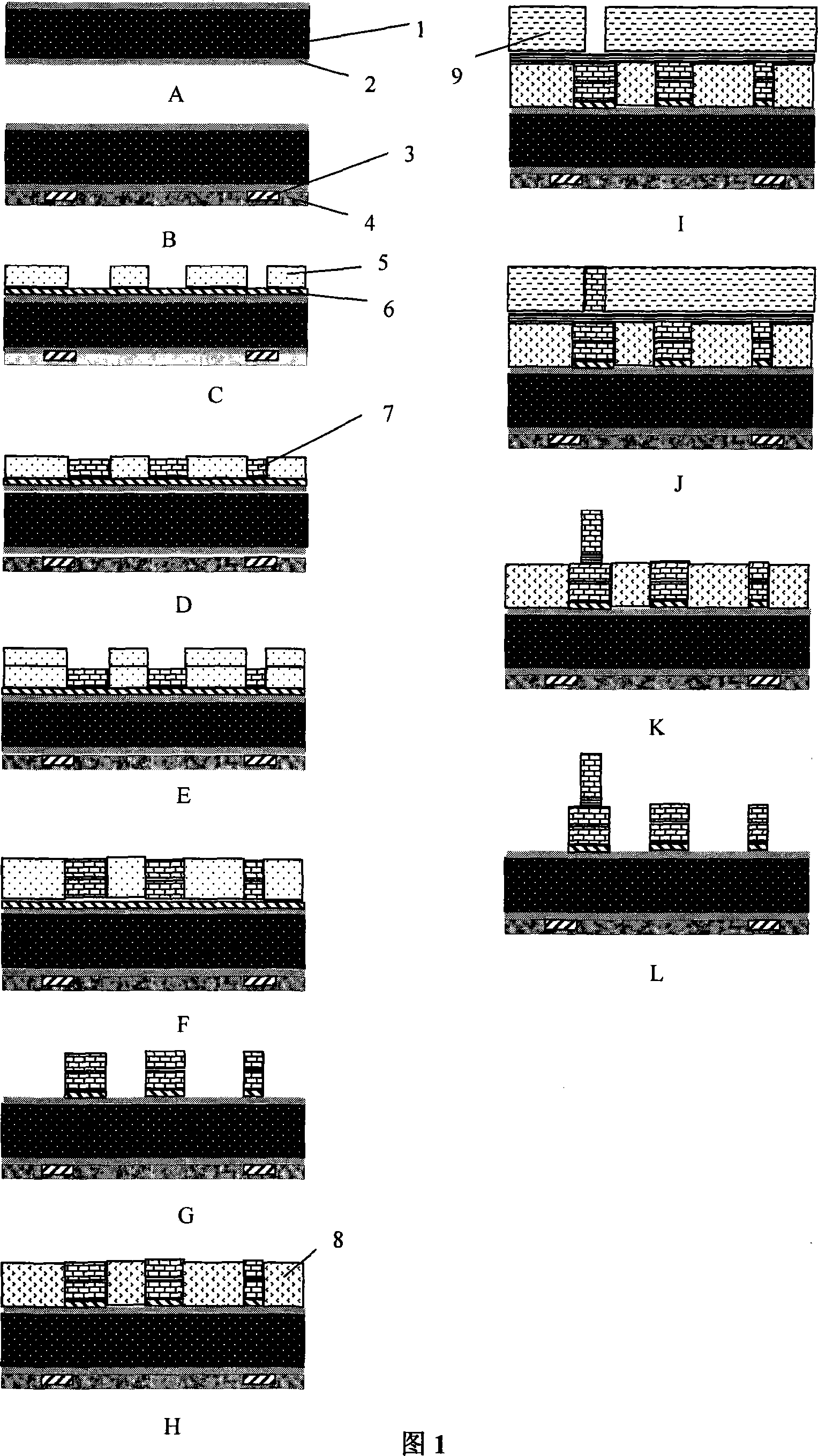
[0019] The embodiments of the present invention are described in detail below in conjunction with the accompanying drawings: this embodiment is implemented on the premise of the technical solution of the present invention, and detailed implementation methods and specific operating procedures are provided, but the protection scope of the present invention is not limited to the following the described embodiment.

[0020] Taking the combination of positive resist AZ P4620 and SU8-100 negative resist process to process the microstructure as an example, the seed layer is made of Cr / Cu metal composite film, the material of the electroplated structural layer is copper (Cu), and a double-sided exposure photolithography machine is used. In the present embodiment, the specific parameter conditions of some processes are: (1) the sputtering seed layer Cr / Cu metal composite film adopts the Z550 type AC and DC magnetron sputtering system of German Leybold-Heraus company, and the basic condi...


PUM


Abstract

The invention discloses a micro-structural realization method on pyrolytic graphite substrate, belonging to a micro electromechanical technical field, the method adopts pyrolytic graphite as the substrate, and then performs the leveling, cleaning, insulating and re-cleaning of the substrate; the back of the pyrolytic graphite substrate is arranged with lithography alignment marks, multi-layer structure or high aspect ratio structure is formed by overlay; the front of the pyrolytic graphite substrate is sprayed with metallic film as seed layer, positive photoresist, lithography and develop are performed, and then electroplating mold is made so as to form an electroplating structural layer, after performing the positive photoresist, lithography and developing twice, positive photoresist is removed, ultrasonic cleaning is performed, and alumina is sprayed, and then the substrate is ground and is cleaned; the alumina is sprayed with the metallic film as the seed layer, and the seed layer is spread with SU8 negative photoresist, after performing the lithography, developing and electroplating, the SU8 negative photoresist is removed and the alumina is removed, so that the high aspect ratio structure is made on the pyrolytic graphite substrate. The invention has novel substrate materials and special processing performance.

Description

technical field [0001] The invention relates to a method in the field of micro-electromechanical technology, in particular to a method for realizing a microstructure on a pyrolytic graphite substrate. Background technique [0002] MEMS is developed with the development of semiconductor integrated circuit microfabrication technology and ultra-precision machining technology. Therefore, in the past few decades, research on the fabrication of micromechanical structures on silicon substrates has been carried out. However, due to the wide variety of MEMS devices and most of them have movable microstructures, it puts forward new requirements in design, materials, processing, system integration, packaging and testing technologies. In this respect, MEMS itself is different from IC. Features, in terms of materials and processing methods, the most typical is non-silicon MEMS, especially the processing of microstructures on glass substrates. The emergence of these non-silicon substrate...

Claims


Application Information

Patent Timeline
IPC IPC(8): B81C1/00
Inventor 张卫平陈文元刘武张忠榕
Owner SHANGHAI JIAO TONG UNIV
Why Eureka
Try Eureka