Method for reducing scratches on surface of epitaxial wafer

A technology for epitaxial wafers and scratches, applied in the direction of electrical components, semiconductor/solid-state device manufacturing, circuits, etc., can solve the problems of increased hydrogen etching rate, fast etching rate, enlarged substrate surface scratches, etc., to reduce and weakening of scratches and reduction of epitaxial defects

Active Publication Date: 2017-05-31
NO 55 INST CHINA ELECTRONIC SCI & TECHNOLOGYGROUP CO LTD
View PDF2 Cites 11 Cited by
  • Summary
  • Abstract
  • Description
  • Claims
  • Application Information

AI Technical Summary

Problems solved by technology

Under the conditions of high temperature, low reaction chamber pressure and large flow rate of hydrogen, the etching rate of hydrogen on the substrate is fast and tends to be anisotropic etching. mark

Method used


Image

  • Method for reducing scratches on surface of epitaxial wafer
  • Method for reducing scratches on surface of epitaxial wafer

Examples


Embodiment Construction

[0017] The technical solutions of the present invention will be further described below in conjunction with the accompanying drawings and embodiments.

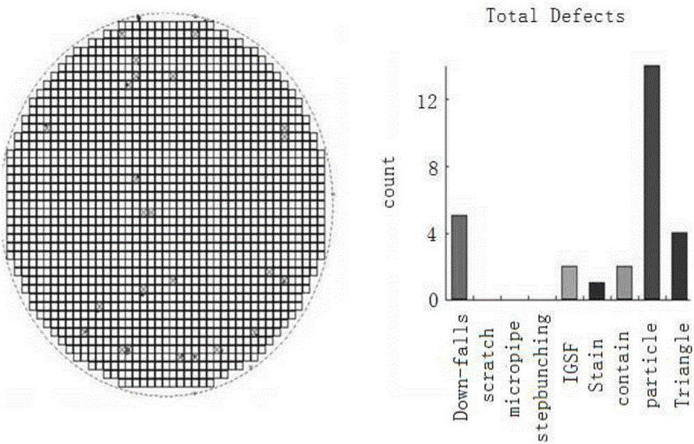
[0018] The method for reducing scratches on the surface of epitaxial wafers described in the present invention is suitable for single-chip epitaxial furnaces and planetary multi-chip silicon carbide epitaxial furnaces, can effectively reduce the number of scratches on the surface of epitaxial wafers, and reduce the number of scratches in the epitaxial layer. Other epitaxial defects derived, this method is compatible with the existing epitaxial process, specifically includes the following steps:

[0019] (1) Place the silicon carbide substrate in the reaction chamber of the SiC epitaxy system, and place it on the graphite base, which has a tantalum carbide coating. The silicon carbide substrate can be selected to be 4° or 8° in the direction of ° silicon carbide substrate;

[0020] (2) Use argon to replace the gas in the reac...


PUM


Abstract

The invention discloses a method for reducing scratches on the surface of an epitaxial wafer. The method comprises the following steps of (1) putting a silicon carbide substrate on a graphite substrate in a reaction chamber of a silicon carbide epitaxial system; (2) replacing a gas in the reaction chamber with argon for multiple times, and then introducing hydrogen into the reaction chamber, gradually increasing the flow of the hydrogen to 20-40L / min, setting the pressure of the reaction chamber to be 700-1,000mbar and gradually heating the reaction chamber to 1400-1500 DEG C; and (3) after reacting a set temperature, keeping all parameters invariable and carrying out in-situ hydrogen etching treatment on the silicon carbide substrate for 10-60 minutes. According to the method disclosed by the invention, the substrate is treated by adopting low-speed hydrogen etching which tends to be isotropic under the conditions of a relatively low temperature, high pressure of the reaction chamber and low-flow hydrogen, so that the scratches on the surface of the substrate can be effectively reduced and weakened, other epitaxial defects derived from the scratches in an epitaxial layer are reduced, the method is compatible with an existing epitaxy process and core process parameters do not need to be modified.

Description

technical field [0001] The invention relates to a method for growing an epitaxial wafer, in particular to a method for reducing scratches on the surface of the epitaxial wafer. Background technique [0002] SiC is a wide-bandgap semiconductor material suitable for the development of high-temperature, high-power, and high-frequency electronic devices, and it is also a high-quality substrate for growing III-VI compound semiconductors. At present, the maximum size of commercial SiC substrates has reached 6 inches, but due to the high mechanical strength and good chemical stability of SiC materials, it is difficult to perform mechanical or chemical polishing like silicon materials. Standard diamond abrasive processing will cause mechanical damage that is invisible to the naked eye. Surface research on SiC substrates has found that there are often many fine scratches on the surface of commercial SiC substrates, and there is a damage layer of about 10 nanometers below the substrat...

Claims


Application Information

Patent Timeline
Patent Type & Authority Applications(China)
IPC IPC(8): H01L21/02
Inventor 李赟
Owner NO 55 INST CHINA ELECTRONIC SCI & TECHNOLOGYGROUP CO LTD
Why Eureka
Try Eureka