Field emission device with carbon nanotubes

a carbon nanotube and emission device technology, applied in the field of field emission devices, can solve the problems of complex cnt field emission arrays, low voltage operation of field emission arrays, and shielding of applied electric fields, and achieve the effects of simple structure, less shielding, and easy production and assembly

Active Publication Date: 2008-01-10
TSINGHUA UNIV +1
View PDF12 Cites 23 Cited by
  • Summary
  • Abstract
  • Description
  • Claims
  • Application Information

AI Technical Summary

Benefits of technology

[0010] An advantage of the electron emitter source is that the CNT electron emitters are less shielded when emitting electrons in that the CNT tips are distributed relatively far away from each other.
[0011] Another advantage is that the electron emitter source is simple in structure and easy to be produced and assembled, thus reducing possibility of impurities to be involved in.
[0012] A further advantage is that the electron emitter source can emit electrons at a relatively lower voltage.
[0013] A still further advantage is that depositing CNTs on metal wires are easier and cheaper than on large size planar surface.
[0014] A yet further advantage is that the field emission device driven with a lower voltage have a longer operation lifetime.

Problems solved by technology

However, tips of adjacent CNTs 11′ that are too close to each other may cause shielding of the applied electric field.
This goes against the demand for operation of field emission arrays at low voltages.
In addition, such a CNT field emission array is complicated and difficult to produce and assemble.
Furthermore, during production and assembly, impurities may become trapped in the CNT field emission array.
This may shorten the useful operating lifetime of the CNT field emission array.

Method used


Image

  • Field emission device with carbon nanotubes
  • Field emission device with carbon nanotubes
  • Field emission device with carbon nanotubes

Examples


Embodiment Construction

[0022] Reference will now be made to the drawings to describe a preferred embodiment of the present invention in detail.

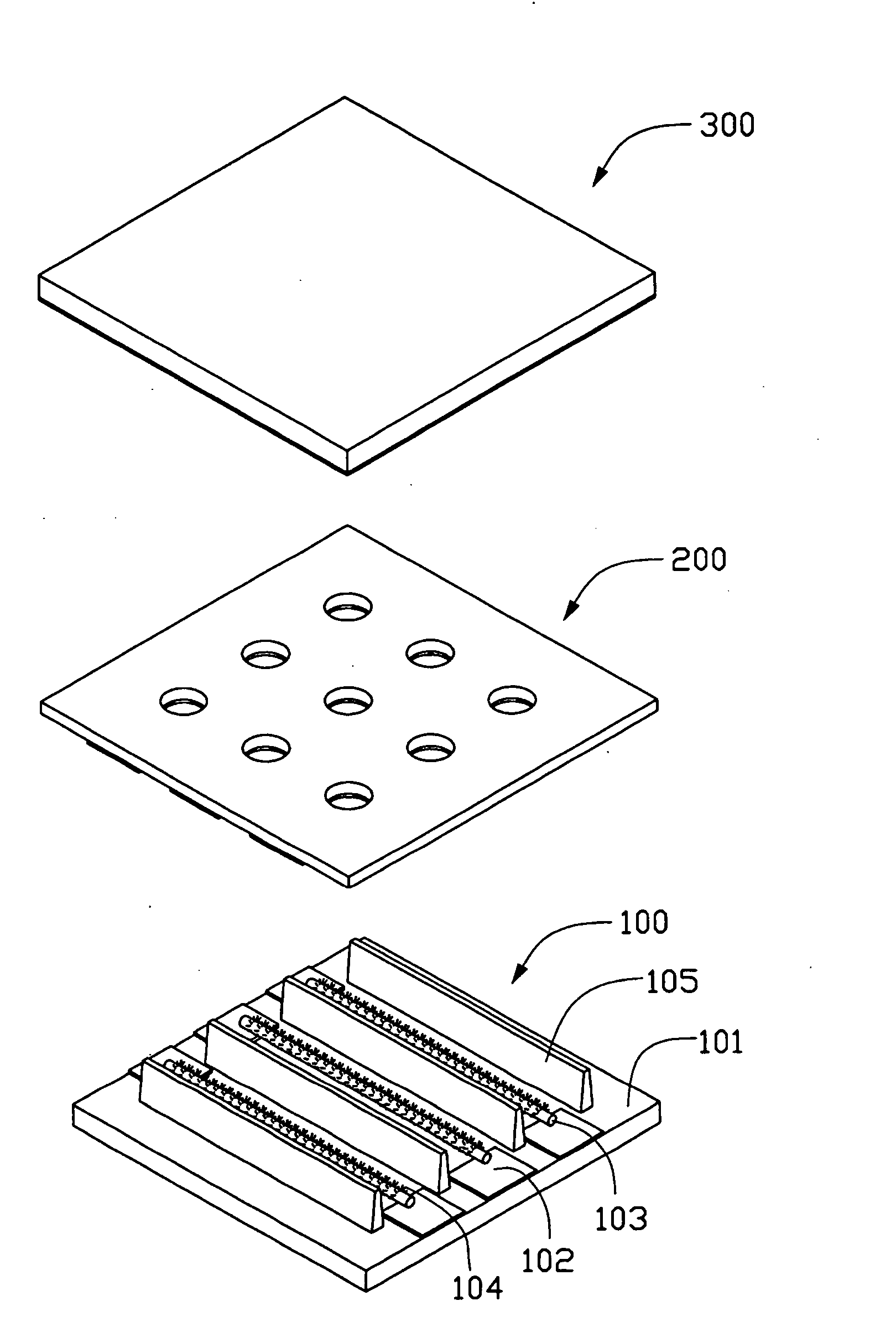
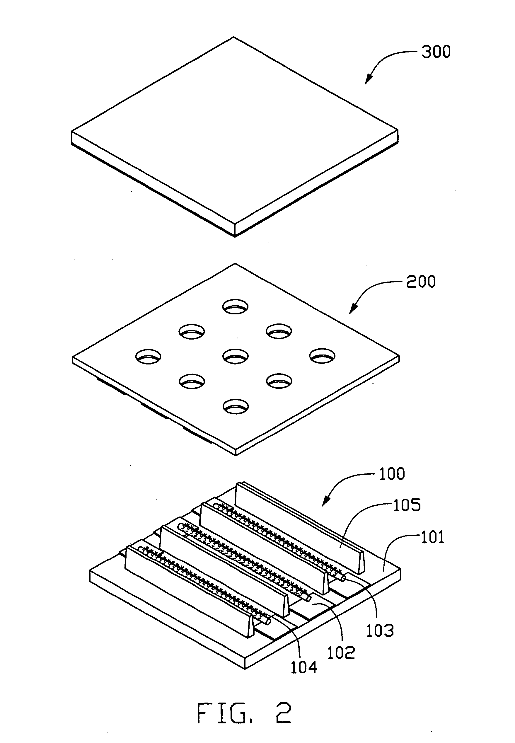
[0023] Referring now to the drawings, and more particularly to FIG. 2, a field emission device includes a CNT electron emitter source 100, a plate-like gate electrode member 200, and a plate-like anode electrode member 300. The gate electrode plate 200 is substantially disposed over the electron emitter source 100, and the anode electrode plate 300 is substantially disposed over the gate electrode plate 200. The electron emitter source 100 includes a dielectric glass substrate 101, a plurality of cathode connectors 102, a plurality of metal wires 103, a plurality of electron emitters 104, and a plurality of dielectric barriers 105. The cathode connectors 102 are distributed along two opposite sides of the dielectric glass substrate 101. The metal wires 103 are arranged parallel to each other. Each metal wire 103 spans between the opposite sides of the dielectric g...


PUM


Abstract

A carbon nanotube (CNT) electron emitter source is provided according to the present invention. The CNT electron emitter source includes a dielectric glass substrate (101), a plurality of cathode connectors (102), a plurality of metal wires (103), a plurality of CNT electron emitters (104) provided on surfaces of the metal wires, and a plurality of dielectric barriers (105). The cathode connectors are distributed along two opposite sides of the dielectric glass substrate. Each of the metal wires has two terminals secured on a pair of corresponding opposite cathode connectors. Each of the metal wires has a substantially protrusive surface, and at least some of the electron emitters discretely extend from the protrusive surface into a space surrounding the metal wire. The dielectric barriers are distributed on the dielectric glass substrate alternately between the metal wires.

Description

BACKGROUND OF THE INVENTION [0001] 1. Field of the Invention [0002] The present invention relates to a field emission device, and more particularly to a field emission device having a carbon nanotube (CNT) electron emitter source. [0003] 2. Prior Art [0004] CNTs were originally produced as by-products of fullerene synthesis. CNTs have remarkable mechanical, electronic, and magnetic properties, which can be varied in principle by varying diameters and chiralities of the CNTs and the number of concentric shells that constitute each CNT. CNTs with extremely small diameters, hollow centers, chemical inertness, and mechanical strength have been used in a vast range of nanotube applications, such as electron field emitters, room-temperature transistors, and vehicles for hydrogen storage. In particular, there has been much effort to develop field emission displays (FEDs) using CNTs. CNT-FEDs have great potential for being applied to emissive devices including flat panel displays, cathode-r...

Claims


Application Information

Patent Timeline
Patent Type & Authority Applications(United States)
IPC IPC(8): H01J1/62
CPCB82Y10/00H01J2201/30469H01J31/127H01J29/04
Inventor WEI, YANGLIU, LIANGFAN, SHOU-SHAN
Owner TSINGHUA UNIV
Why Eureka
Try Eureka