Process for improving the reliability of interconnect structures and resulting structure

a technology of interconnect structure and reliability, applied in the field of integrated circuit structure and formation methods, can solve the problems of increasing line-to-line capacitance, limiting the speed of the integrated circuit by interconnect capacitance, and not generally applying the scaling factor to line width and line-to-line spacing, so as to improve the diffusion barrier layer, reduce electrical migration, and reduce the porosity

Inactive Publication Date: 2008-01-17
TAIWAN SEMICON MFG CO LTD
View PDF11 Cites 14 Cited by
  • Summary
  • Abstract
  • Description
  • Claims
  • Application Information

AI Technical Summary

Benefits of technology

[0011]The advantageous features of the present invention include an improved diffusion barrier layer due to smaller porosity when the diffusion barrier layer is formed and reduced electrical migration due to a prolonged electrical migration path.

Problems solved by technology

However, the same scaling factor applied to line width and line-to-line spacing is not generally applied to interconnect line thickness due to the need to maintain minimum current-carrying capacity.
In addition, the number of lines that are needed to interconnect the increased number of devices also increases, resulting in an increase in the line-to-line capacitance.
In some high-speed circuits, this interconnect capacitance can be the limiting factor in the speed of the integrated circuit.
However, it has been found that use of such low dielectric constant (low-k) materials is often problematic.
Due to the different voltages in the metal lines, leakage current may exist between the metal lines, which causes electrical migration.
As a result, the reliability of the integrated circuit is adversely affected, and the mean time to failure (MTTF) is reduced.

Method used


Image

  • Process for improving the reliability of interconnect structures and resulting structure
  • Process for improving the reliability of interconnect structures and resulting structure
  • Process for improving the reliability of interconnect structures and resulting structure

Examples


Embodiment Construction

[0015]The making and using of the presently preferred embodiments are discussed in detail below. It should be appreciated, however, that the present invention provides many applicable inventive concepts that can be embodied in a wide variety of specific contexts. The specific embodiments discussed are merely illustrative of specific ways to make and use the invention, and do not limit the scope of the invention.

[0016]The intermediate stages of manufacturing a preferred embodiment of the present invention are illustrated in FIGS. 2 through 8B. Throughout the various views and illustrative embodiments of the present invention, like reference numbers are used to designate like elements.

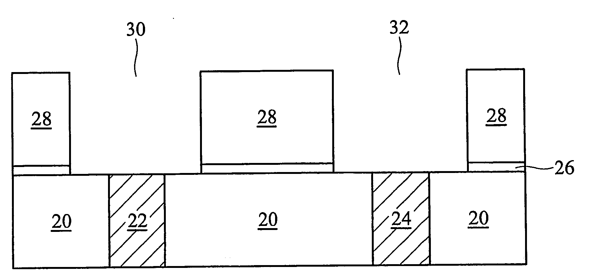
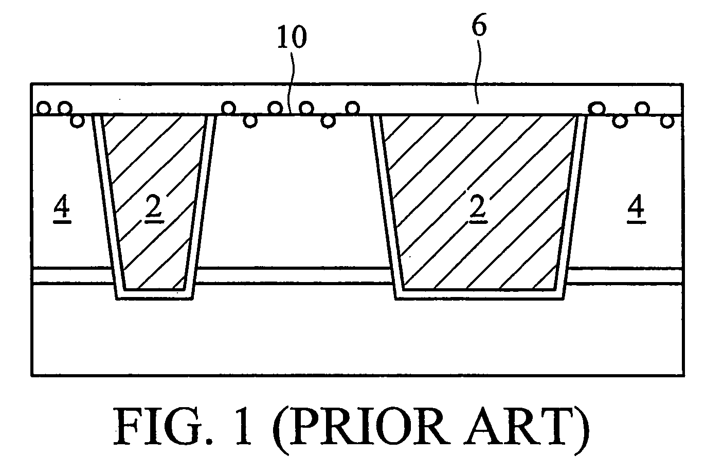
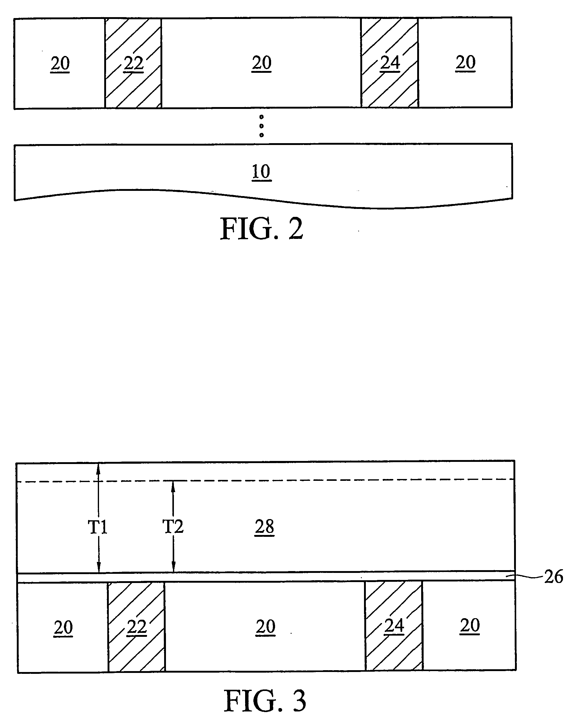
[0017]FIG. 2 illustrates a substrate 10, a dielectric layer 20 over substrate 10 and two conductive features 22 and 24 formed in dielectric layer 20. Conductive features 22 and 24 are preferably metal lines comprising copper, tungsten, aluminum, silver, gold, and the like. They can also be formed of othe...


PUM

PropertyMeasurementUnit
shrinkage ratesaaaaaaaaaa
wavelengthaaaaaaaaaa

Abstract

An interconnect structure of an integrated circuit having improved reliability and a method for forming the same are provided. The method includes providing a substrate, forming a dielectric layer overlying the substrate, performing a first shrinking process, wherein the dielectric layer shrinks and has a first shrinkage rate, forming a conductive feature in the dielectric layer after the step of performing the first shrinking process, and performing a second shrinking process after the step of forming the conductive feature, wherein the dielectric layer substantially shrinks and has a second shrinkage rate.

Description

TECHNICAL FIELD[0001]This invention relates generally to integrated circuits, and more particularly to the structure and formation methods of interconnect structures in integrated circuits.BACKGROUND[0002]As advances in processing technology allow for an increasing number of devices to be fabricated on a single integrated circuit (IC), the surface area or size of each individual device on the IC is scaled down or reduced. Conductive lines or interconnect structures that electrically couple such individual devices are also scaled. However, the same scaling factor applied to line width and line-to-line spacing is not generally applied to interconnect line thickness due to the need to maintain minimum current-carrying capacity. Thus, interconnect lines are often thicker than those for which the scaling factor employed for the line width would predict.[0003]Adjacent interconnect lines form parasitic capacitors. The plate area of each plate of the capacitor formed is the product of the l...

Claims


Application Information

Patent Timeline
Patent Type & Authority Applications(United States)
IPC IPC(8): H01L21/4763
CPCH01L21/7682H01L21/76829H01L21/76828H01L2221/1047
Inventor CHEN, HSIEN-WEILIN, JIAN-HONGLEE, TZU-LI
Owner TAIWAN SEMICON MFG CO LTD
Why Eureka
Try Eureka