Methods for fabricating field emission display devices

a field emission display and field emission technology, applied in the field can solve the problems of poor display quality, less space occupied by projection tvs, and large display area, and achieve the effects of improving the uniformity of field emission display devices, preventing arching, and high-efficiency environmental surface treatment methods

Inactive Publication Date: 2008-01-17
IND TECH RES INST
View PDF6 Cites 6 Cited by
  • Summary
  • Abstract
  • Description
  • Claims
  • Application Information

AI Technical Summary

Benefits of technology

[0017]Accordingly, the invention is related to a surface treatment method for FED devices. By thoroughly removing impurities and contaminants from the field emitters, uniformity of the field emission display device is improved. High-efficiency environmentally friendly surface treatment methods are provided. A plurality of substrates can be treated simultaneously without producing additional contaminants, thereby preventing arching due to high operation voltage and improving stability of the FED device in a high vacuum.

Problems solved by technology

Compared with conventional large scale display devices, CRT displays have excellent display quality but occupy a large amount of space.
Projection TVs occupy less space but offer poor display quality.
Plasma display panel (PDP) displays exhibit lighter, thinner features and can be fabricated by screen printing, nonetheless, they require high power consumption.
Field emitters formed by semiconductor thin film process, however, require high cost apparatus and are difficult to achieve on a large scale.
Some impurity residues may remain on the surface of the electron emission layer, creating porous structure, affecting field emission efficiency.
The field emission structure 70A, however, exhibits degraded field emission efficiency.
Moreover, the adhesive tape 30 cannot be reused, increasing production cost.
The surface of the field emitters may be damaged during release of the adhesive tape 30.
The organic residue from the adhesive tape 30 may result in the field emitter arching at high operating voltages, degrading properties of the FED devices.
The roller used in the rubbing, however, may leave residual dust or impurities on the surface of the field emitters, which can result in the field emitter arching at high operation voltage, degrading properties of the FED devices.
Some particles may, however, remain, degrading properties of the FED devices.
The field emission display device activated by laser treatment can, however, be damaged by undesirable heating.
Moreover, if the laser treatment is performed after the field emission display device is assembled, it is difficult to address and align the laser source, inter alia, for high definition FED devices, resulting in intricate fabrication procedures and reduced throughput.

Method used


Image

  • Methods for fabricating field emission display devices
  • Methods for fabricating field emission display devices
  • Methods for fabricating field emission display devices

Examples


Embodiment Construction

[0030]The following description is of the mode of carrying out the invention. This description is made for the purpose of illustrating the general principles of the invention and should not be taken in a limiting sense. The scope of the invention is best determined by reference to the appended claims.

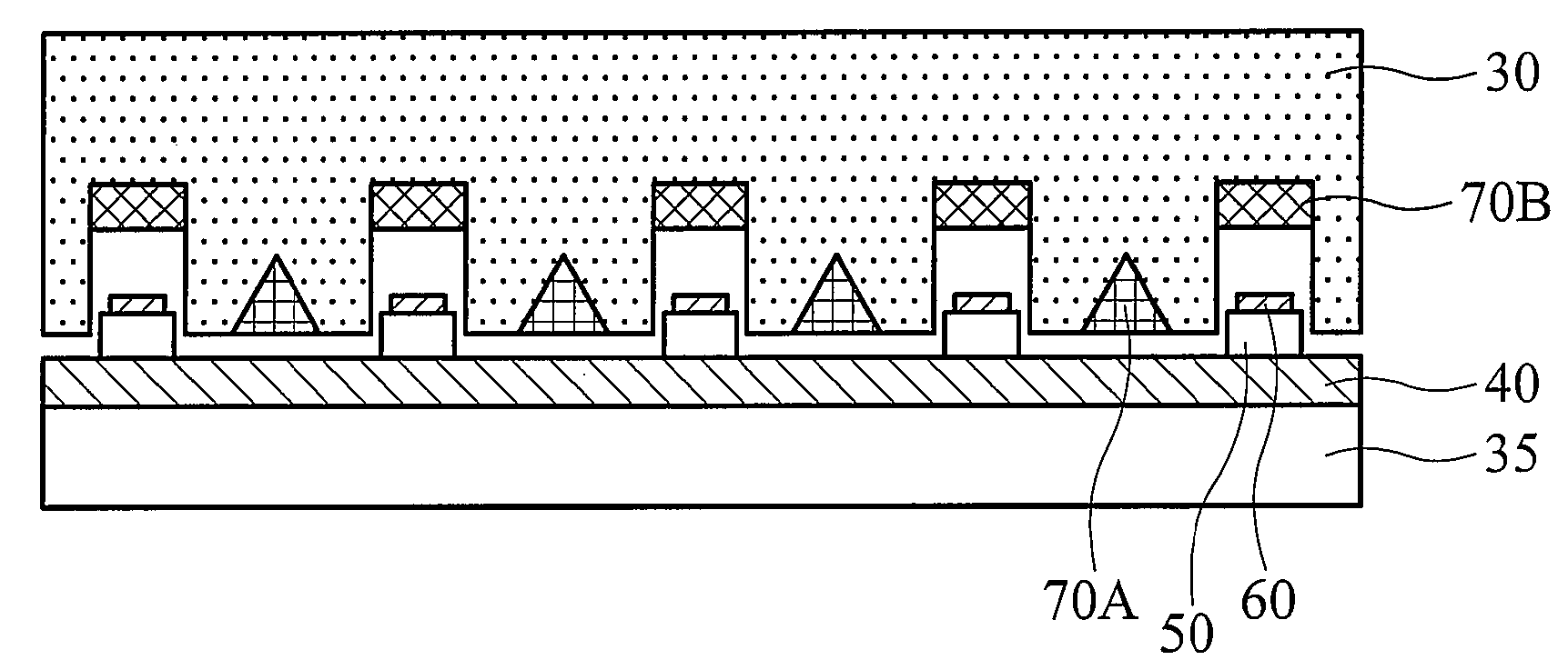
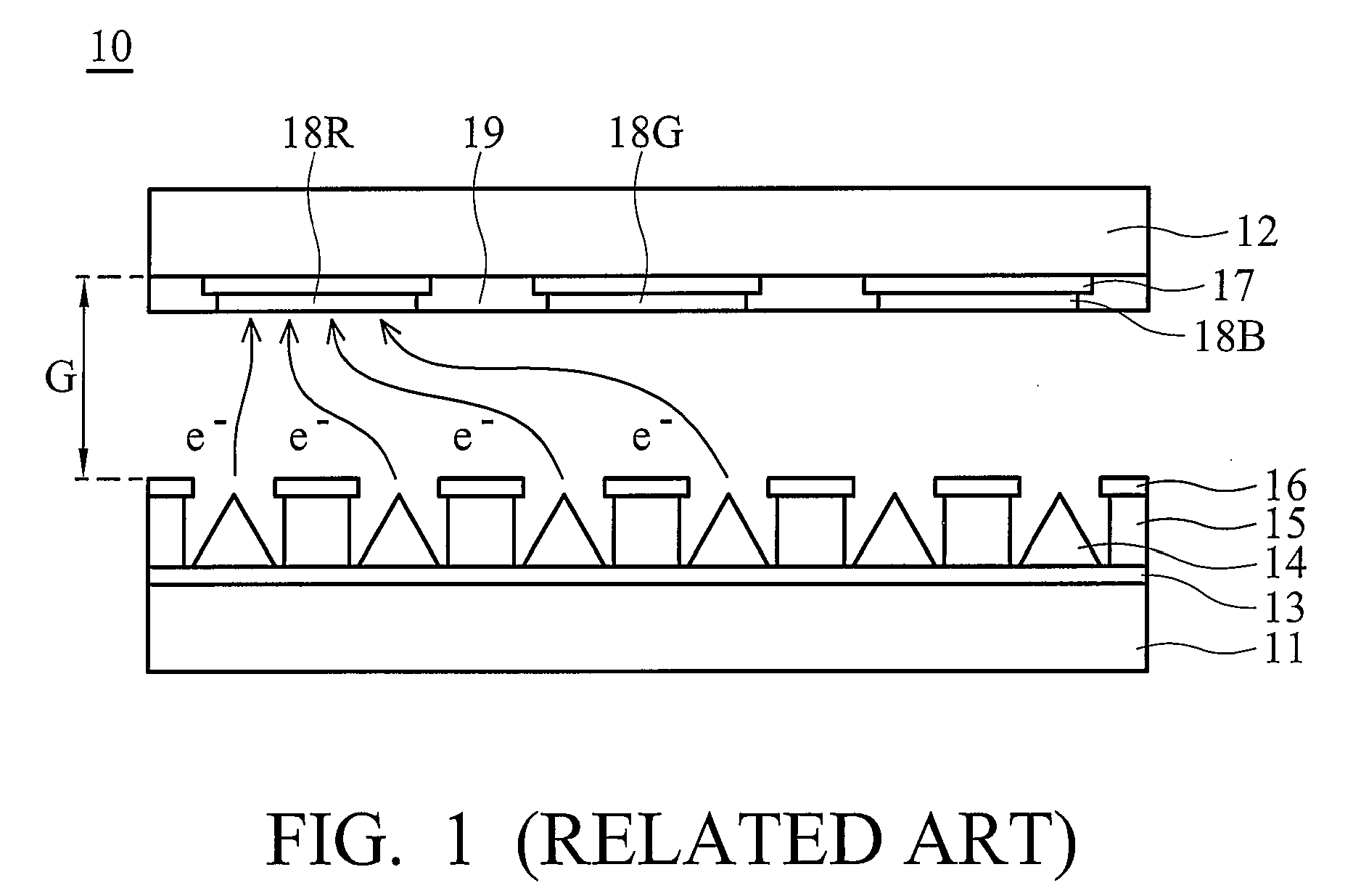
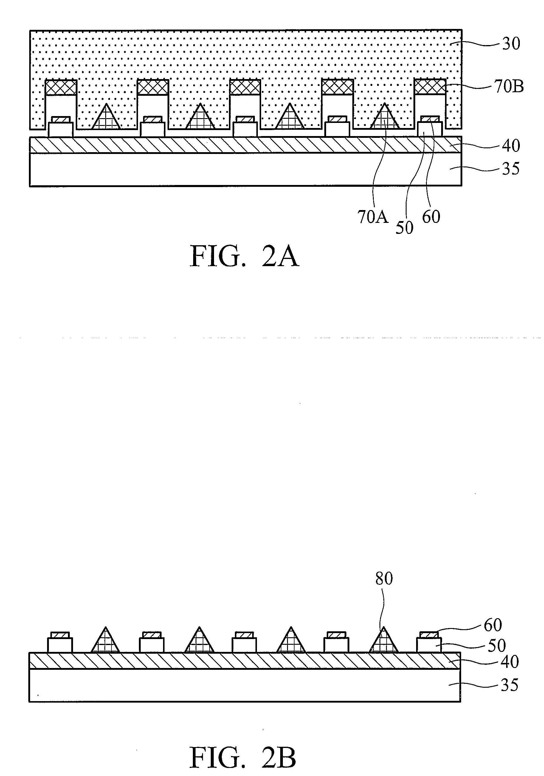
[0031]The invention is related to an FED panel and surface treatment methods thereof. The cathode substrate is activated by methods combining free radical oxidization and supercritical carbon dioxide fluid cleaning to improve uniformity and stability of the FED panel. A plurality of cathode substrates can be treated simultaneously to purify and modify surface properties of the field emitters without producing potential contaminants. Furthermore, surface properties of carbon nanotube powders can be modified according to a embodiment, thereby improving uniformity and stability of the FED panel.

[0032]FIG. 4A is a fabrication flowchart of a FED panel according to an embodiment of the invent...


PUM


Abstract

Methods for fabricating field emission display devices. A first substrate is provided. A cathode structure is formed on the first substrate. A surface treatment procedure is performed on the first substrate with cathode structure thereon. A second substrate opposing the first substrate is provided and assembled in vacuum with a wall rib therebetween. The surface treatment procedure includes free radical oxidization and a supercritical CO2 fluid cleaning.

Description

BACKGROUND OF THE INVENTION[0001]1. Field of the Invention[0002]The invention relates to field emission display (FED) devices, and in particular to methods for fabricating field emission display devices.[0003]2. Description of the Related Art[0004]Field emission display (FED) devices are panelized conventional cathode ray tube (CRT) displays. Using screen printing technology, large scale FED devices can be achieved. Conventional larger scale FED devices provide low volume, light weight, low power consumption, excellent image quality, and are applicable to a variety of electronic and communication devices. Carbon nanotube or other nano-scale field emitters have benefits such as low threshold field, high emission current density, and high stability due to lower threshold voltage, higher light efficiency, higher viewing angle, and lower power consumption.[0005]Compared with conventional large scale display devices, CRT displays have excellent display quality but occupy a large amount o...

Claims


Application Information

Patent Timeline
Patent Type & Authority Applications(United States)
IPC IPC(8): H01J9/02
CPCH01J31/127H01J9/025
Inventor JIANG, YAU-CHENHSIAO, MING-CHUNCHEN, YING-HSIENCHEN, KUANG-CHUNG
Owner IND TECH RES INST
Why Eureka
Try Eureka