
Novel metal nanoparticle and formation of conductive pattern using the same

a metal nanoparticle and conductive pattern technology, applied in the field of new metal nanoparticles and a method for forming a conductive pattern using the same, can solve the problems of difficult control and arrangement of microparticles uniformly, difficulty in the regulation of space regularity or molecular orientation, unstability, etc., and achieve the effect of easy to achieve the arrangement of nanoparticles

Inactive Publication Date: 2008-01-24
SAMSUNG ELECTRONICS CO LTD
View PDF2 Cites 26 Cited by
  • Summary
  • Abstract
  • Description
  • Claims
  • Application Information

AI Technical Summary

Benefits of technology

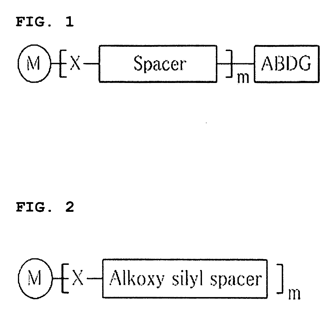
[0010]Accordingly, the present inventors have endeavored to overcome the above-mentioned problems and have developed a metal nanoparticle which is prepared by forming a self-assembled monolayer including a terminal reactive group on the surface thereof, and introducing a functional group capable of being removed by the action of an acid or an base into the terminal reactive group. The self-assembled monolayer is made from a thiol, an isocyanide, an amine, a carboxylate or a phosphate compound having the terminal reactive group, or built up of a thiol compound and the like having no terminal reactive group followed by introducing the terminal reactive group thereinto. As a result, the present inventors have found that using such metal nanoparticle is easy to achieve nanoparticle arrangement throughout a large area. Also, it is made possible to form a conductive pattern including the metal nanoparticle on the surface of various kinds of substrates through a conventional photolithography process, without performing an additional sputtering or etching process.
[0011]It is, therefore, an object of the invention to provide a novel metal nanoparticle capable of easily forming a large area film or an ultramicro pattern, and a method for forming a pattern using the same.

Problems solved by technology

However, it is very difficult to control and arrange microparticles uniformly in order to apply the metal nanoparticle to a film or a pattern.
However, when using the metal nanoparticle including the well-known self-assembled monolayer, there are several problems such as difficulties in the regulation of the space regularity or molecular orientation, unstability, defects, surface ordering control, and aggregation of the metal nanoparticle when fabricated into a thin film.
For the above reasons, therefore, it is impossible to easily prepare a large area film or an ultramicro pattern which has even limited industrial applicability.

Method used


Image

  • Novel metal nanoparticle and formation of conductive pattern using the same
  • Novel metal nanoparticle and formation of conductive pattern using the same
  • Novel metal nanoparticle and formation of conductive pattern using the same

Examples


example 1

Introduction of an Acid-Degradable Group into the Surface of a Gold Nanoparticle

[0097]After 0.2 g of the gold nanoparticle obtained in Preparative Example 1 was mixed with 50 M of a mixture of concentrated sulfuric acid and 30% hydrogen peroxide (1:1), the mixture was gently stirred for 20 minutes, diluted with 250 M of distilled water, and was filtered with a 0.2 μm filter. The filtered residue obtained as described above was washed with 50 M of methanol five times and dried in a 160° C. oven for 5 hours. Then, 0.1 g of the dried gold nanoparticle was added to 200 M of toluene together with 1.3 g of 4-cyanophenol and was stirred for 72 hours. The product generated above was filtered with a 0.2 μm filter, was washed with THF twice, and was dried in a 30° C. oven under reduced pressure. After 0.02 g of the resulting product was added to 2 M of fresh toluene, the mixture was subjected to ultrasonication for 10 minutes, was added with 0.40 M of triethylamine and 0.22 M of triethylaceth...

example 2

Introduction of an Acid-Degradable Group into the Surface of a Silver Nanoparticle

[0098]The silver nanoparticle having an acid-degradable group introduced into the surface thereof was obtained according to the same method as described in Example 1 except that 0.2 g of the silver nanoparticle prepared in Preparative Example 2 was employed instead of the gold nanoparticle.

example 3

Introduction of an Acid-Degradable Group into the Surface of a Copper Nanoparticle

[0099]The copper nanoparticle having an acid-degradable group introduced into the surface thereof was obtained according to the same method as described in Example 1 except that 0.2 g of the copper nanoparticle prepared in Preparative Example 3 was employed instead of the gold nanoparticle.


PUM

PropertyMeasurementUnit
Percent by massaaaaaaaaaa

Abstract

A metal nanoparticle which is prepared by forming a self-assembled monolayer including a terminal reactive group on the surface thereof, and introducing a functional group capable of being removed by the action of an acid or an base into the terminal reactive group wherein the self-assembled monolayer is built up of a thiol, an isocyanide, an amine, a carboxylate or a phosphate compound having the terminal reactive group, or built up of a thiol, an isocyanide, an amine, a carboxylate or a phosphate compound having no terminal reactive group followed by introducing the terminal reactive group thereto; and a method for forming a conductive pattern using the same are provided. Since the metal nanoparticle of exemplary embodiments of the present invention can easily form a high conductive film or a high conductive pattern through photo-irradiation and photo-degradation and randomly regulate its conductivity when occasions demand, it can be advantageously applied to an antistatic washable sticky film, antistatic shoes, a conductive polyurethane printer roller, an electromagnetic interference shielding, and the like.

Description

BACKGROUND OF THE DISCLOSURE[0001]This non-provisional application claims priority under 35 U.S.C. § 119(a) on Korean Patent Application No. 2006-68501 filed on Jul. 21, 2006 which is herein incorporated by reference.[0002]1. Field of the Disclosure[0003]Exemplary embodiments of the present invention relate to a novel metal nanoparticle and a method for forming a conductive pattern using the same. More particularly, exemplary embodiments of the present invention are directed to a novel metal nanoparticle, which is prepared by forming a self-assembled monolayer including a terminal reactive group on the surface thereof, and introducing a functional group capable of being removed by the action of an acid or a base into the terminal reactive group, and a method for forming a conductive pattern using the same. The self-assembled monolayer is built up of a thiol, an isocyanide, an amine, a carboxylate or a phosphate compound having the terminal reactive group, or is built up of a thiol c...

Claims


Application Information

Patent Timeline
IPC IPC(8): G03C1/72B32B15/02
CPCB05D1/185C03C17/06G03F7/0047H05K3/02Y10T428/2991H05K2203/0514Y10S977/779Y10S977/778Y10S977/777H05K2201/0257B82B1/00B82B3/00B82Y40/00
Inventor PARK, JONG JINSHIN, DONG WOOKIM, SUNG WOONG
Owner SAMSUNG ELECTRONICS CO LTD
Learn More