

Methods of forming a doped semiconductor thin film, doped semiconductor thin film structures, doped silane compositions, and methods of making such compositions
a technology of semiconductor thin films and compositions, applied in the direction of coatings, electrical appliances, basic electric elements, etc., can solve the problems of not quite reproducible, disappointing properties of thin films formed from such compounds, and difficult to make semiconducting thin films of commercial qualities and quantities, etc., to reduce the volatility of compositions, increase the average molecular weight, and increase the viscosity
- Summary
- Abstract
- Description
- Claims
- Application Information
AI Technical Summary
Benefits of technology
Problems solved by technology
Method used
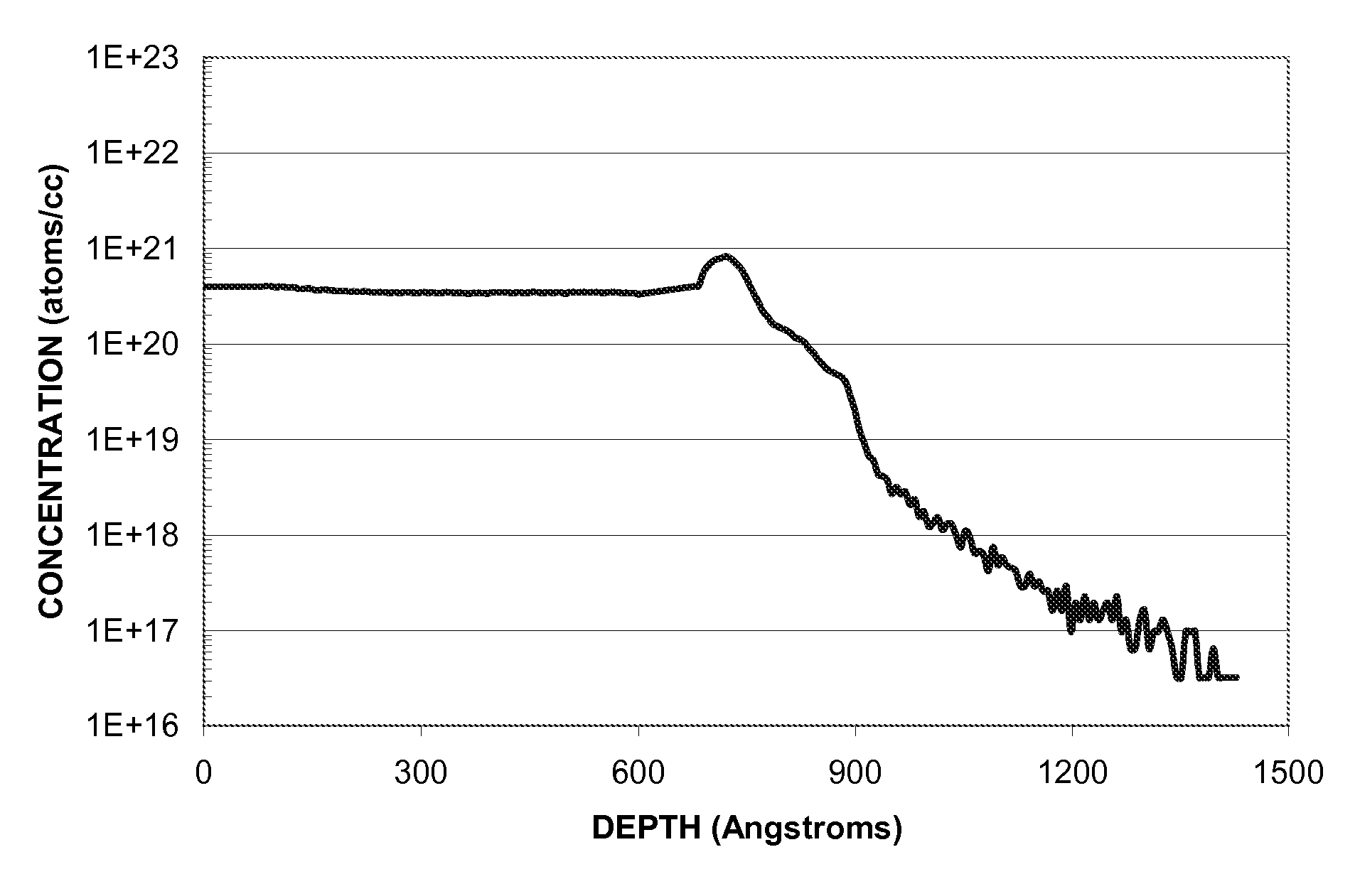
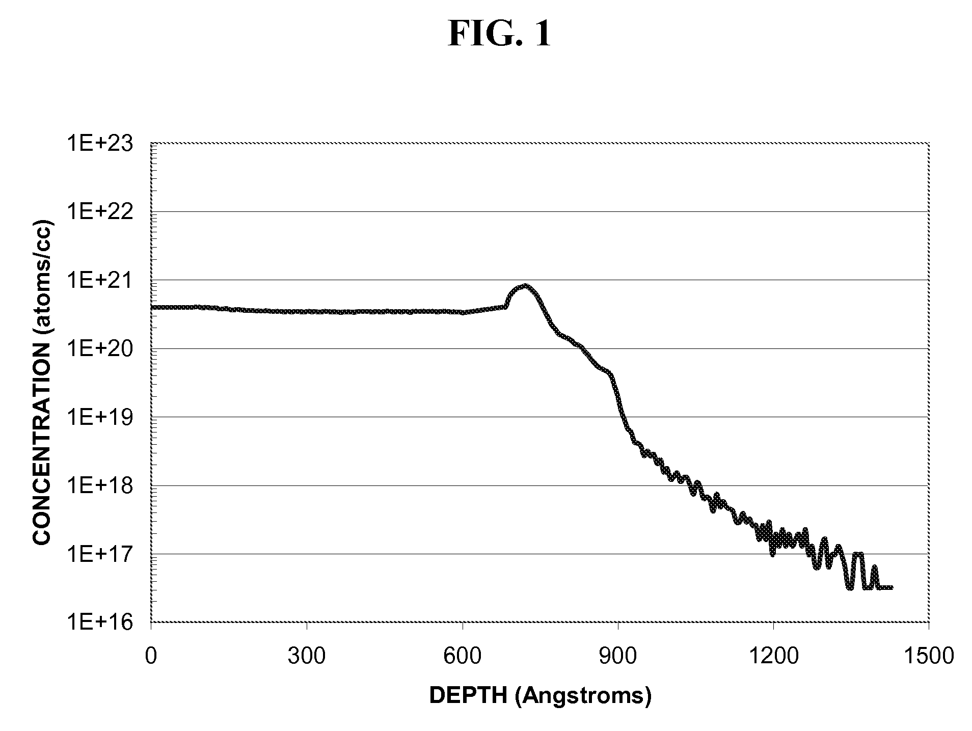
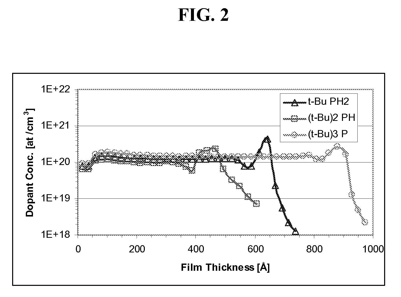
Image

Examples
examples
Synthesis of cyclo(phenylphospha)tetrasilane
[0097] In a 1 L 4-neck flask equipped with addition funnels, a thermometer and a gas dispersion tube, 10 g of nonaphenylcyclophosphatetrasilane obtained as described in copending U.S. application Ser. No. ______, (Attorney Docket No. IDR0301, entitled “Heterocyclic Semiconductor Precursor Compounds, Compositions Containing the Same, and Methods of Making Such Compounds and Compositions” and filed concurrently herewith, the relevant portions of which are incorporated herein by reference) and 0.3 g freshly sublimed AlCl3 are suspended in 200 ml of dry toluene. Under vigorous stirring, dry HCl gas is bubbled through this suspension at ambient temperature until an almost colorless to yellow solution is obtained. Under continuous HCl bubbling, the solution is stirred for 5-8 hrs.
[0098] 50 mL of a 1M ethereal solution of LiAlH4 (Aldrich) is added under vigorous stirring to the toluene solution at 0° C. The resulting suspension is further stirr...
PUM
| Property | Measurement | Unit |
|---|---|---|
| vol % | aaaaa | aaaaa |
| vol % | aaaaa | aaaaa |
| time | aaaaa | aaaaa |
Abstract
Description
Claims
Application Information