Photovoltaic element and fabrication method thereof

a technology of photovoltaic elements and fabrication methods, applied in the field of photovoltaic elements, can solve problems such as warpage or fracture of elements, reducing the mounting strength between the tab and the collector electrode, and problematically reducing reliability or an output, so as to suppress the effect of reducing an outpu

Inactive Publication Date: 2008-01-31
SANYO ELECTRIC CO LTD
View PDF6 Cites 75 Cited by
  • Summary
  • Abstract
  • Description
  • Claims
  • Application Information

AI Technical Summary

Benefits of technology

[0027]In accordance with the present invention, a photovoltaic element can be fabricated which allows use of...

Problems solved by technology

This produces a mechanical stress in the photovoltaic element to result in the occurrence of warpage or fracture of the element, which has been a problem.
However, it generally lowers mounting strength between the tab and collector electrodes to problematically reduce reliability or ...

Method used


Image

  • Photovoltaic element and fabrication method thereof
  • Photovoltaic element and fabrication method thereof
  • Photovoltaic element and fabrication method thereof

Examples


Embodiment Construction

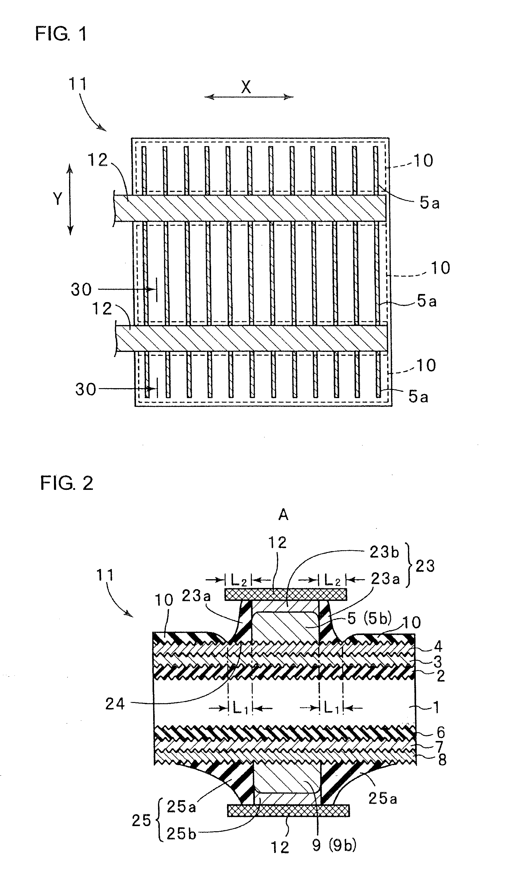
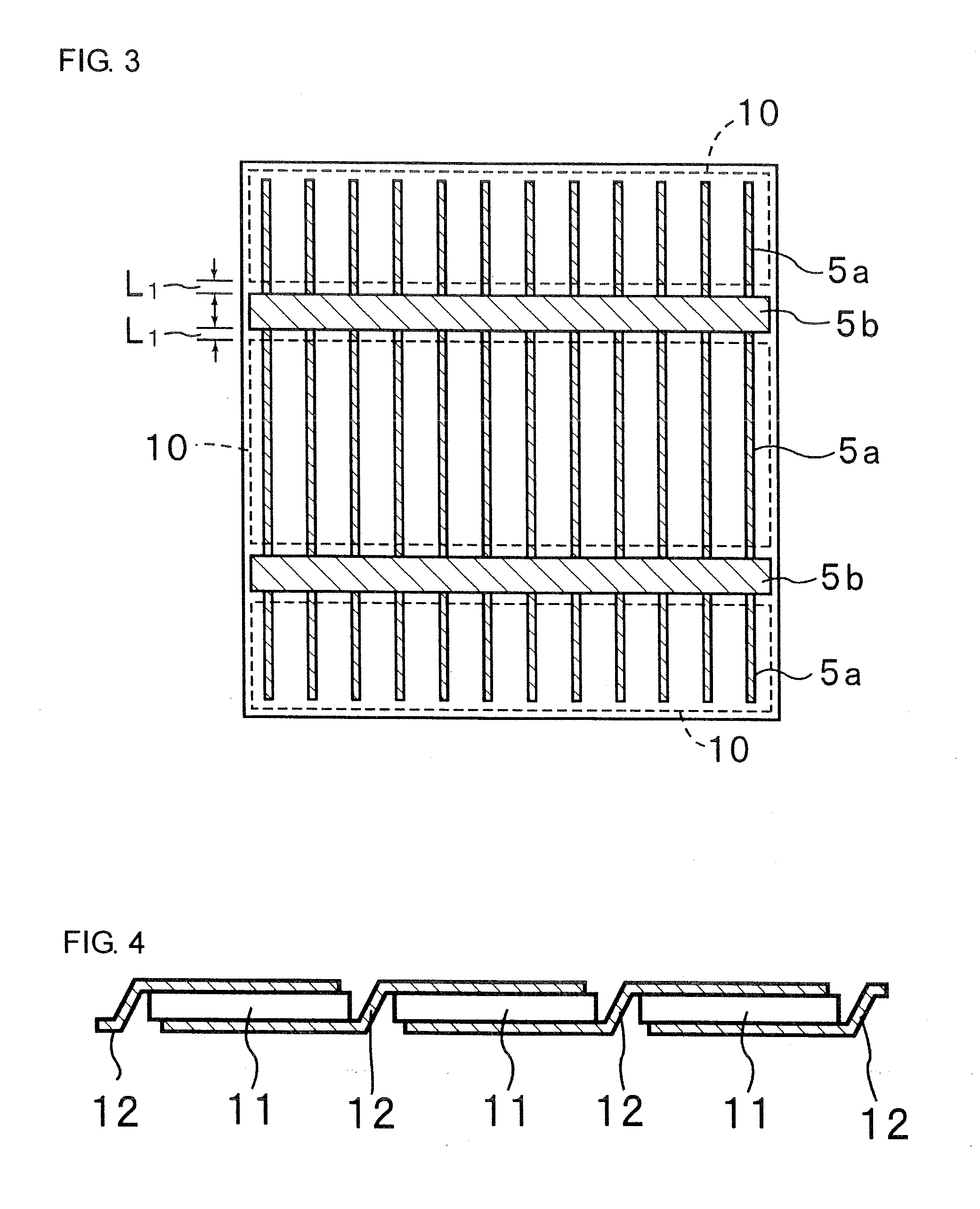
[0034]FIG. 1 is a plan view illustrating an embodiment of a photovoltaic element in accordance with the present invention and FIG. 2 is a sectional view taken along the line 30-30 of FIG. 1.

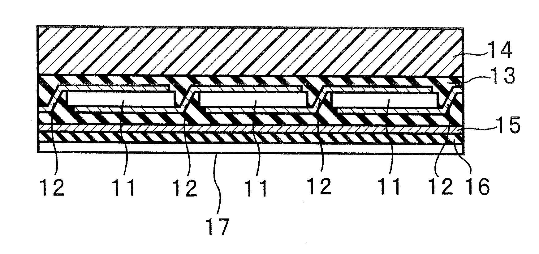
[0035]As shown in FIG. 2, an embodiment of a photovoltaic element 11 in accordance with the present invention includes an n-type single crystal silicon substrate 1 having a thickness of about 140 μm-about 300 μm, a substantially intrinsic i-type amorphous silicon layer 2 formed on a top surface (light-receiving surface) of the silicon substrate 1 and having a thickness of about 5 nm-about 20 nm, and a p-type amorphous silicon layer 3 formed on the i-type amorphous silicon layer 2 and having a thickness of about 5 nm-about 20 nm. Formed on the p-type amorphous silicon layer 3 is an ITO translucent conductive film 4 having a thickness of about 30 nm-about 150 nm.

[0036]A collector electrode 5 is formed on a predetermined region of the translucent conductive film 4 by thermosetting a silver (Ag) past...


PUM


Abstract

A photovoltaic element is obtained which allows use of a low-melting solder and can suppress reduction in reliability and output thereof due to mechanical stress or water intrusion.
The photovoltaic element has a photoelectric conversion layer and a collector electrode provided on at least one surface of the photoelectric conversion layer. Characteristically, a collector electrode covering layer for covering a surface of the collector electrode is provided and a tab electrode for electrical connection to an exterior electrode is provided on a top surface of the collector electrode through the collector electrode covering layer. A portion of the collector electrode covering layer that lies between the tab electrode and collector electrode comprises a solder layer and another portion of the collector electrode covering layer that covers a lateral surface of the collector electrode comprises a thermosetting resin layer.

Description

BACKGROUND OF THE INVENTION[0001]1. Technical Field[0002]The present invention relates to a photovoltaic element and a fabrication method thereof.[0003]2. Description of Related Art[0004]A photovoltaic element is known which has a translucent conductive film, such as of ITO (indium tin oxide), formed on a surface of a photoelectric conversion layer for collection of a current generated in the conversion layer, and a collector electrode formed on the conductive film for passing the current to the outside. As the collector electrode, a finger electrode configured to extend from one end of an element surface to the other end thereof and comprising plural fingers spaced apart at regular intervals and a bus bar electrode integrally formed with the finger electrode for further collection of the current collected in the finger electrode are generally formed.[0005]A tab electrode is generally mounted to the collector electrode for carrying the current collected in the collector electrode to...

Claims


Application Information

Patent Timeline
IPC IPC(8): H01L31/0216B05D5/12H01L31/04H01L31/18
CPCY02E10/50H01L31/0512H01L31/02167
Inventor TERADA, NORIHIROONO, MASAYOSHIOKAMOTO, SHINGO
Owner SANYO ELECTRIC CO LTD
Why Eureka
Try Eureka