
Electrolytic plating method

a technology of electrolysis and plating, applied in the direction of semiconductor/solid-state device details, manufacturing tools, transportation and packaging, etc., can solve the problems of inability to control the electrical quantity of the inside of the hole, the inability to completely fill the inside of the non-through hole the difficulty of filling the inside of the non-through hole completely with plated metal without leaving, etc., to achieve excellent filling performance and excellent smoothness of the plated surfa

Inactive Publication Date: 2008-01-31
NIPPON MACDERMID
View PDF7 Cites 18 Cited by
  • Summary
  • Abstract
  • Description
  • Claims
  • Application Information

AI Technical Summary

Benefits of technology

[0006]This invention has been accomplished in view of the above-mentioned point. It is an object of this invention to provide an electrolytic plating method which enables efficiently and consistently to attain excellent filling performance of plated metal into non-through holes on the substrate to be plated and excellent smoothness of plated surface under various plating condition and various composition of plating solution and further enables to achieve satisfactory covering of plating on the surface of substrate and within through holes.SUMMARY OF THE INVENTION

Problems solved by technology

However, in direct current (DC) plating, as the deposition rate of plating depends on only the distance between a substrate to be plated and a counter electrode based on the shape of substrate, the deposition rate of plating at the mouth of hole and that at the inside of hole cannot be controlled electrically (in terms of the quantity of electricity) by a preset electric current.
Therefore it is difficult to fill the inside of non-through hole completely with plated metal without leaving any void or recess within the hole.
Besides, the plated surface by pulse plating usually becomes rough and uneven, which affects the formation of circuits and the assembly of parts.
In this method, however, DC plating is used only for the purpose of smoothing the uneven surface by pulse plating and the filling of plated metal into non-through holes entirely depends on the properties of pulse plating.
Not only this is insufficient in point of productivity, but also it is difficult to simultaneously attain the satisfactory covering of plating within through holes (this type of holes, including the through holes in question, may hereinafter be referred to as “through holes” in a broad sense) in the case of printed circuit boards with both through holes and non-through holes coexisting.
More particularly, in case of filling up non-through holes in accordance with conventional electrolytic plating methods, the composition of plating solution and the plating condition actually applicable are extremely limited.

Method used


Image

  • Electrolytic plating method
  • Electrolytic plating method

Examples


example 1

Influence of Pulse Plating on the Fill Performance of Plating in Non-Through Holes

[0036]

Composition of plating solutionCopper sulfate pentahydrate80 g / LSulfuric acid210 g / LChloride ion60 mg / LPolyethylene glycol800 mg / LSPS (sodium bis-3-sulfopropyl disulfide)5 mg / LCounter electrodeSoluble electrodeCondition of pulse platingCurrent density1.0 A / dm2IR / IF ratio3 / 1Forward current time20 msecReverse current time1 msecPlating time0~112 minCondition of DC platingCurrent density1.0 A / dm2Plating time0~112 minTotal plating thickness25 μm

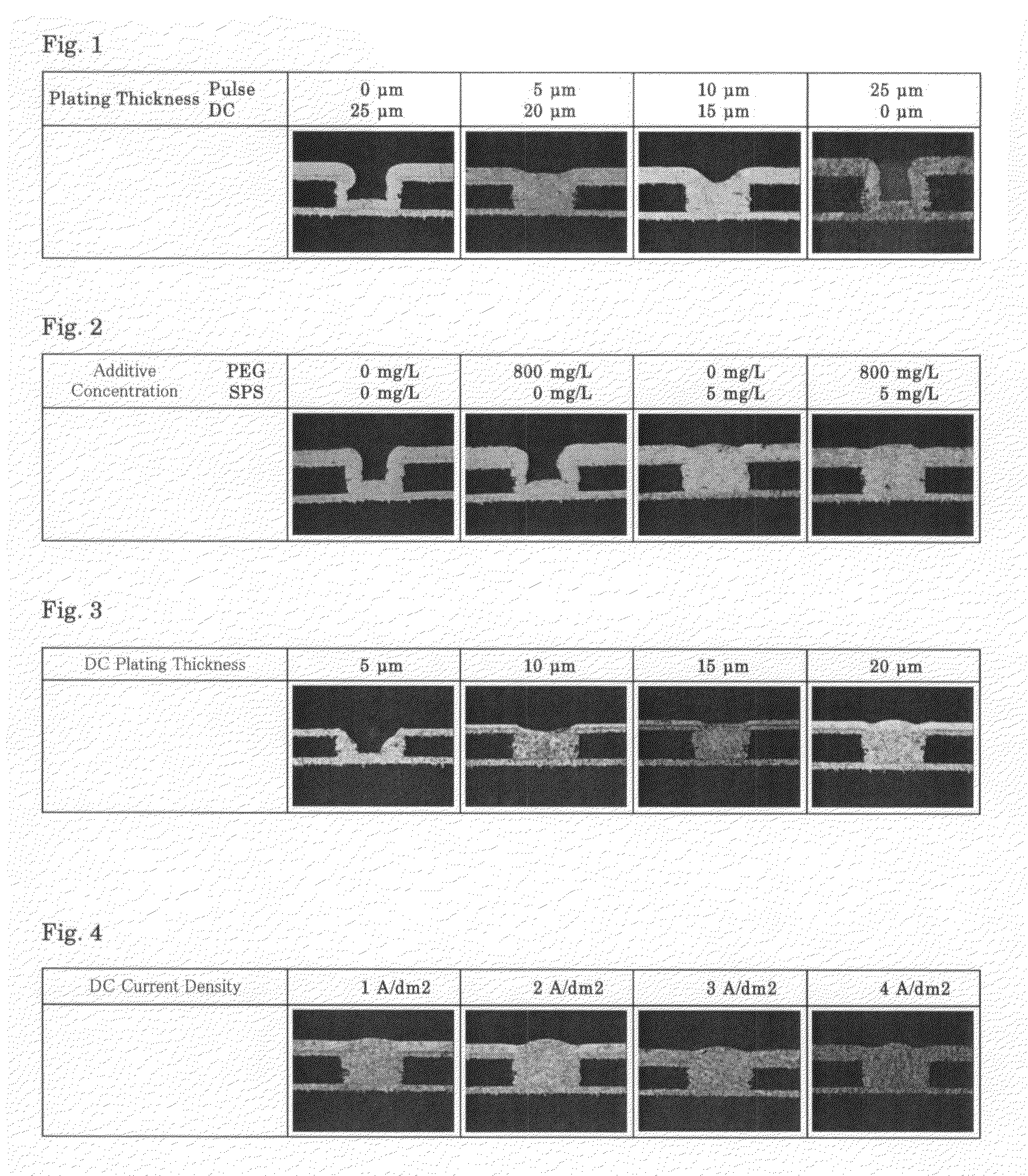
[0037]FIG. 1 shows cross sections of blind via holes plated in Example 1. When the total plating thickness on the surface was at 25 μm, it was impossible, by only pulse plating or only DC plating, to fill up the inside of holes, but when pulse plating was followed by DC plating, it was possible to fill up the inside of holes. Besides, the smaller the pulse plating thickness became, the more satisfactory the fill performance became. It is seen that in the method...

example 2

Influence of Plating Solution Additives on the Fill Performance of Plating in Non-Through Holes

[0038]

Composition of plating solutionCopper sulfate pentahydrate150 g / LSulfuric acid100 g / LChloride ion60 mg / LPolyethylene glycol0 or 800 mg / LSPS (sodium bis-3-sulfopropyl disulfide)0 or 5 mg / LCounter electrodeSoluble electrodeCondition of pulse platingCurrent density2.0 A / dm2IR / IF ratio3 / 1Forward current time20 msecReverse current time1 msecPlating time10 minCondition of DC platingCurrent density2.0 A / dm2Plating time46 minTotal plating thickness25 μm

[0039]FIG. 2 shows cross sections of blind via holes plated in Example 2. Of the plating solution additives, polyethylene glycol is an inhibitor (also called suppressor, wetter, or carrier) and SPS is an accelerator. With a plating solution containing SPS, the blind via holes could be completely filled with plating, but in the absence of SPS it was impossible to fill up the holes.

example 3

Influence of Thickness of DC Plating on the Fill Performance of Plating in Non-Through Holes)

[0040]

Composition of plating solutionCopper sulfate pentahydrate150 g / LSulfuric acid100 g / LChloride ion60 mg / LPolyethylene glycol800 mg / LSPS (sodium bis-3-sulfopropyl disulfide)5 mg / LCounter electrodeInsoluble electrodeCondition of pulse platingCurrent density1.0 A / dm2IR / IF ratio3 / 1Forward current time20 msecReverse current time1 msecPlating time10 minCondition of DC platingCurrent density1.0 A / dm2Plating time0~90 minTotal plating thickness0~20 μm

[0041]FIG. 3 shows cross sections of blind via holes plated in Example 3. Since DC plating grows at the bottom edge of the blind via hole, it is seen that the hole can be filled up completely without forming any void in the hole.


PUM

PropertyMeasurementUnit
thicknessaaaaaaaaaa
concentrationaaaaaaaaaa
current densityaaaaaaaaaa

Abstract

A novel electrolytic plating method suitable for filling non-through holes with metal is disclosed. The electrolytic plating method uses a plating solution containing additives such as a surfactant, a brightening agent and a smoothing agent and includes pulse plating for controlling adsorption and desorption of tie additives on the surface and in the non-through holes of substrate and subsequent DC plating for filling up the non-through holes with metal.

Description

FIELD OF THE INVENTION[0001]This invention relates to a novel electrolytic plating method for filling up non-through holes. The method is applicable, for example, to printed circuit boards and semiconductor wafers used in electronic devices or the like.BACKGROUND OF THE INVENTION[0002]To meet the recent demand for higher function and downsizing of electronic devices, a technology to fabricate printed circuit boards for high dense assembly is required as well as downsizing of electronic parts such as semiconductors and chip parts. An example of such printed circuit boards is build-up printed circuit boards wherein layers are successfully stacked after the circuit is formed on each layer and are electrically connected through blind via holes (this type of holes may hereinafter be referred to as “non-through holes” in a broad sense, including a blind via hole). In this connection, for the purpose of increasing the density of circuits and assembled parts by mounting on the blind via hol...

Claims


Application Information

Patent Timeline
Patent Type & Authority Applications(United States)
IPC IPC(8): H05K1/09C25D3/38H01L23/00
CPCC25D3/38C25D5/18H01L21/2885H01L21/76877H05K3/421Y10T428/12229H05K2201/09563H05K2203/1476H05K2203/1492C25D7/123H05K3/423C25D5/627C25D5/611
Inventor NISHU, KEISUKEIIJIMA, MORIOANDO, NAOMI
Owner NIPPON MACDERMID
Learn More