Semiconductor integrated circuit including a malfunction detection circuit, and a design method for the same
a technology of integrated circuits and malfunction detection, applied in pulse manipulation, pulse technique, instruments, etc., can solve problems such as data loss, data reset, data loss, etc., and achieve the effect of efficient design
- Summary
- Abstract
- Description
- Claims
- Application Information
AI Technical Summary
Benefits of technology
Problems solved by technology
Method used
Image

Examples
embodiment 1
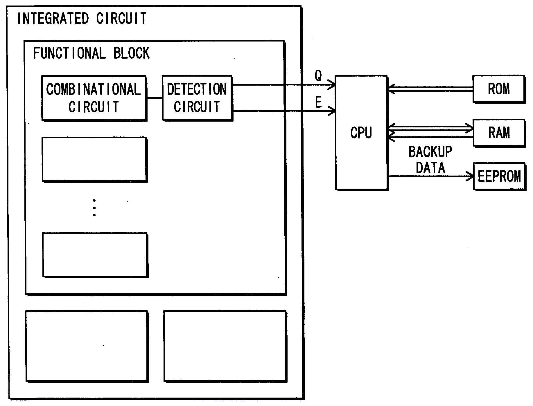
[0102]FIG. 1 shows an overall structure of a semiconductor integrated circuit pertaining to embodiment 1 of the present invention. The semiconductor integrated circuit is constituted from a plurality of functional blocks that are separated according to function, and a plurality of combinational circuits are disposed in each of the functional blocks. If a malfunction due to a temperature variation around a certain combinational circuit in a functional block is to be detected, a malfunction detection circuit is disposed in a latter stage of the combinational circuit. The malfunction detection circuit outputs a malfunction detection signal E that is separate from a signal Q that realizes the normal function of the semiconductor integrated circuit, thereby enabling a CPU (Central Processing Unit) to execute a malfunction countermeasure. For example, when reading data from a RAM (Read Only Memory) or reading / writing data from / to a RAM (Random Access Memory) during normal functioning, the...
embodiment 2
[0153]Setup Error Detection
[0154]FIG. 12 shows a flip-flop 500 used by a malfunction detection circuit of a semiconductor integrated circuit pertaining to embodiment 2 of the present invention, where the flip-flop 500 detects a setup error. The flip-flop 500 has the same circuit structure as after the combinational circuit 104 of FIG. 2, with the addition of a buffer gate cluster 501. Operations of the flip-flop 500 shown in FIG. 12 during normal functioning and during a malfunction are the same as shown by the timing charts of FIGS. 3 and 4 described in embodiment 1, with the exceptions that the internal flip-flops 105 and 108 are driven by a clock CK, and the internal flip-flop 106 is driven by a clock obtained as a result of the buffer gate cluster 501 delaying the clock CK by ΔT1. Accordingly, the flip-flop 500 always outputs “L” as a detection result E during normal functioning, and outputs “H” as a detection result E during a malfunction, thereby enabling detecting a malfuncti...
embodiment 3
[0163]FIG. 16 shows an overview of a malfunction detection circuit of a semiconductor integrated circuit pertaining to embodiment 3 of the present invention. As shown in FIG. 16, a semiconductor integrated circuit 1001 is constituted from, for example, the three functional blocks 1002, 1003 and 1004. Among the flip-flops constituting each of the functional blocks 1002, 1003 and 1004, flip-flops 1005, 1007 and 1009 respectively thereof have the longest setup times, and flip-flops 1006, 1008 and 1010 have the longest hold times. The malfunction detection circuits described in embodiments 1 and 2 are disposed in the flip-flops that have the longest setup times and hold times in the functional blocks.
[0164]According to this structure, disposing at least two malfunction detection circuits in the semiconductor integrated circuit enables detecting a circuit malfunction due to a temperature variation inside or outside the semiconductor chip.
PUM
 Abstract
Description
Claims
Application Information
 - R&D
- Intellectual Property
- Life Sciences
- Materials
- Tech Scout
- Unparalleled Data Quality
- Higher Quality Content
- 60% Fewer Hallucinations
Browse by: Latest US Patents, China's latest patents, Technical Efficacy Thesaurus, Application Domain, Technology Topic, Popular Technical Reports.
© 2025 PatSnap. All rights reserved.Legal|Privacy policy|Modern Slavery Act Transparency Statement|Sitemap|About US| Contact US: help@patsnap.com