Power amplifier circuit for peak envelope modulation of high frequency signal

a power amplifier and high frequency signal technology, applied in the field of radio frequency (rf) transmitters, can solve the problems of reducing the power consumption of passive devices, affecting the performance of amplitude modulation, and affecting the quality of amplitude modulation, so as to and reduce the power loss and signal distortion

Active Publication Date: 2008-01-31
SAMSUNG ELECTRONICS CO LTD
View PDF8 Cites 17 Cited by
  • Summary
  • Abstract
  • Description
  • Claims
  • Application Information

AI Technical Summary

Benefits of technology

[0012]The present invention provides a power amplifier circuit which can control a voltage to be supplied to a power amplification end by classifying an envelope of an input high frequency signal into a high level and a low level using a passive device such as a transformer, to reduce a power loss and signal distortion in a transmitter of a wireless communication system.
[0013]The present invention also provides a method of amplifying a power of a high frequency signal, which can reduce a power loss and signal distortion by detecting an envelope of an input high frequency signal, extracting a peak envelope greater than a predetermined size from the detected envelope via a limiter, and supplying the peak envelope, as a supply voltage, to a power amplification end via a transformer.

Problems solved by technology

As described above, since an active device, such as the transistor, is utilized at the end of the power voltage control circuit 110 for signal mixing, a comparatively great amount of power loss and signal distortion occurs.
However, like a waveform 220, the output signal POUT is distorted in ranges where a signal level is greater than a predetermined level and less than the predetermined level due to non-linearity of the active device.
Also, since the active device has a comparatively greater resistance than a passive device, power consumption is greater than the passive device.
As shown in FIG. 4, since the transistor Q1 generally operates around an operating point PP, a power loss increases.

Method used


Image

  • Power amplifier circuit for peak envelope modulation of high frequency signal
  • Power amplifier circuit for peak envelope modulation of high frequency signal
  • Power amplifier circuit for peak envelope modulation of high frequency signal

Examples


Embodiment Construction

[0025]Reference will now be made in detail to exemplary embodiments of the present invention, examples of which are illustrated in the accompanying drawings, wherein like reference numerals refer to like elements throughout. The exemplary embodiments are described below to explain the present invention by referring to the figures.

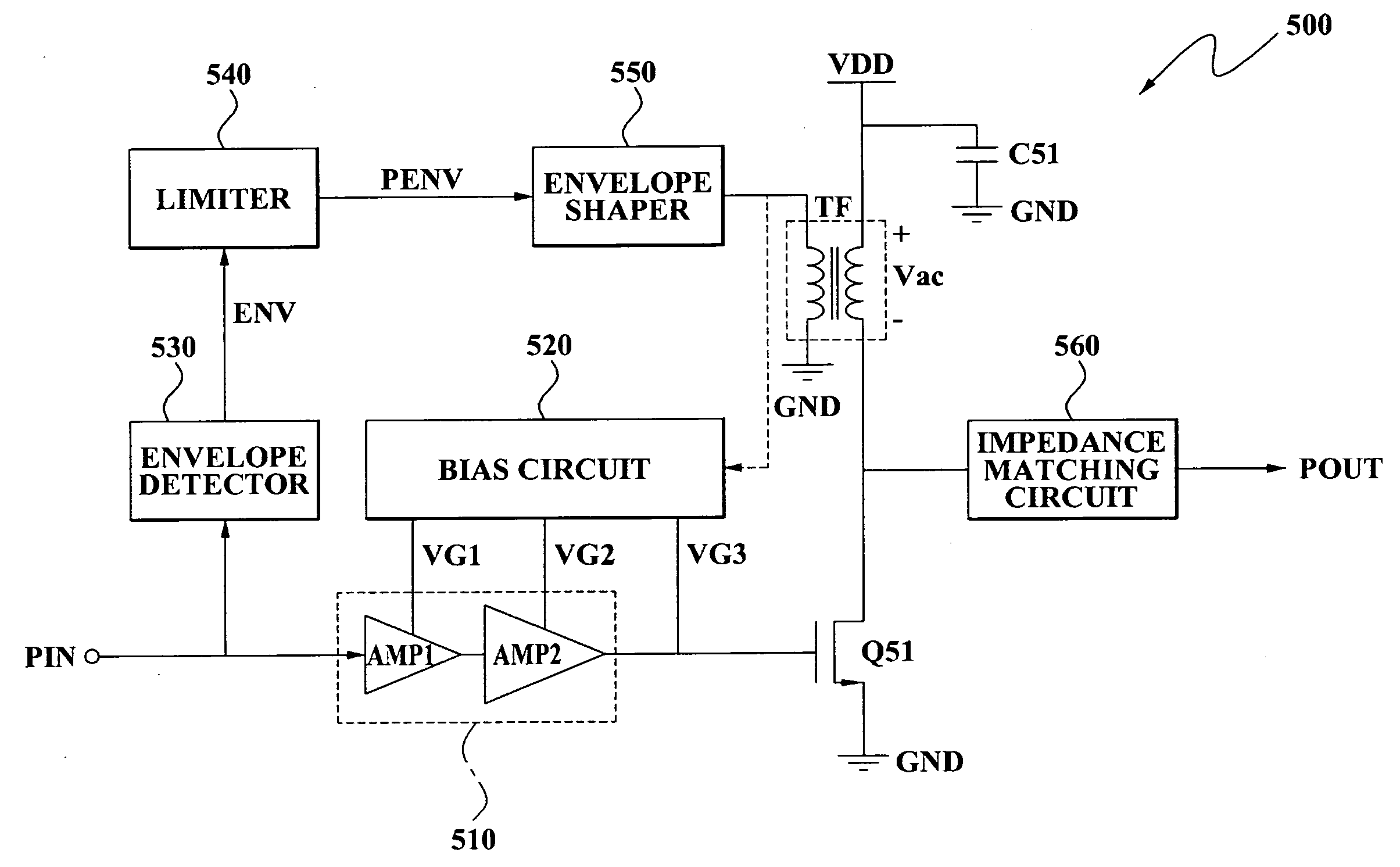
[0026]FIG. 5 is a diagram illustrating a power amplifier circuit 500 according to an exemplary embodiment of the present invention. Referring to FIG. 5, the power amplifier circuit 500 includes a driver stage 510, a power amplification transistor Q51, a transformer TF, a bias circuit 520, an envelope detector 530, a limiter 540, an envelope shaper 550, an impendence matching circuit 560, and a capacitor C51. Signal waveforms as shown in FIGS. 6 and 7 are utilized for explaining operations of the power amplifier circuit 500.

[0027]The power amplifier circuit 500 according to the present exemplary embodiment receives an input high frequency signal PIN, and gen...


PUM


Abstract

A power amplifier circuit for peak envelope modulation of a high frequency signal is provided. The power amplifier circuit includes a transformer which receives a first signal greater than a predetermined level of an envelope of a carrier signal to generate a transformed signal, and a transistor which operates based on the transformed signal, receives a second signal, which is generated based on the carrier signal and has a direct current component, and amplifies the second signal according to the transformed signal to output an output signal.

Description

CROSS-REFERENCE TO RELATED APPLICATION[0001]This application claims priority from Korean Patent Application No. 10-2006-0070733, filed on Jul. 27, 2006, in the Korean Intellectual Property Office, the entire disclosure of which is incorporated herein by reference.BACKGROUND OF THE INVENTION[0002]1. Field of the Invention[0003]Apparatuses consistent with the present invention relate to a radio frequency (RF) transmitter, and more particularly, to a power amplifier circuit which can effectively amplify a power by classifying an envelope of an input high frequency signal that corresponds to a high level and a low level, and controlling a voltage to be supplied to a power amplification end.[0004]2. Description of Related Art[0005]In a transmitter of a system for high speed wireless communication such as a mobile phone, a digital multimedia broadcasting (DMB) phone, a personal digital assistant (PDA), and the like, various transmission schemes including an envelope modulation, for exampl...

Claims


Application Information

Patent Timeline
Patent Type & Authority Applications(United States)
IPC IPC(8): H03G3/20
CPCH03C1/36H03F1/0205H03F1/0266H03F3/245H03F2200/541H03F2200/387H03F2200/408H03F2200/451H03F2200/102H03F1/02H03F3/21
Inventor KIM, SEUNG WOO
Owner SAMSUNG ELECTRONICS CO LTD
Why Eureka
Try Eureka