Semiconductor memory device

a memory device and semiconductor technology, applied in the direction of information storage, static storage, digital storage, etc., can solve the problems of increasing the capacity load of the read line rbl and the write bit line wbl with increasing the memory size, and achieve the effect of speeding up the read and write operations and reducing the power consumption of the semiconductor memory devi

Inactive Publication Date: 2008-01-31
SONY CORP
View PDF3 Cites 38 Cited by
  • Summary
  • Abstract
  • Description
  • Claims
  • Application Information

AI Technical Summary

Benefits of technology

[0068]The present invention enables the speedup of read and write operations and the reduction of the power consumption in the semiconductor memory device having memory cells performing the data input (write) and data output (read) at different nodes.

Problems solved by technology

However, the parasitic resistances and capacity loads of the read line RBL and the write bit line WBL increases with increase of a memory size.

Method used


Image

  • Semiconductor memory device
  • Semiconductor memory device
  • Semiconductor memory device

Examples


Embodiment Construction

[0097]An example of a semiconductor memory device according to an embodiment of the present invention is described below with reference to the related drawings.

[0098]FIG. 8 is a general block diagram illustrating a semiconductor memory device.

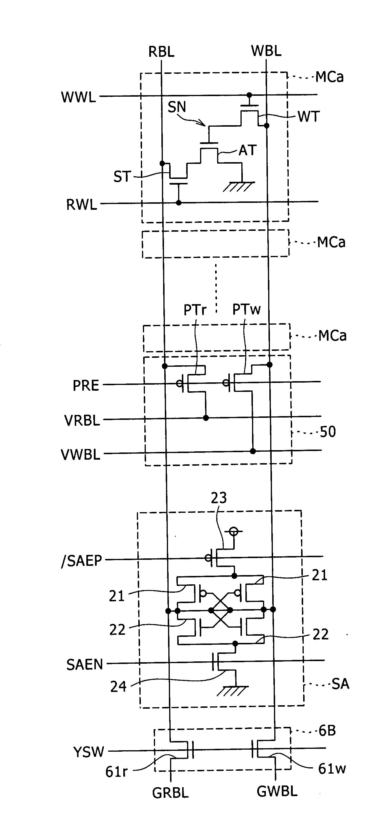
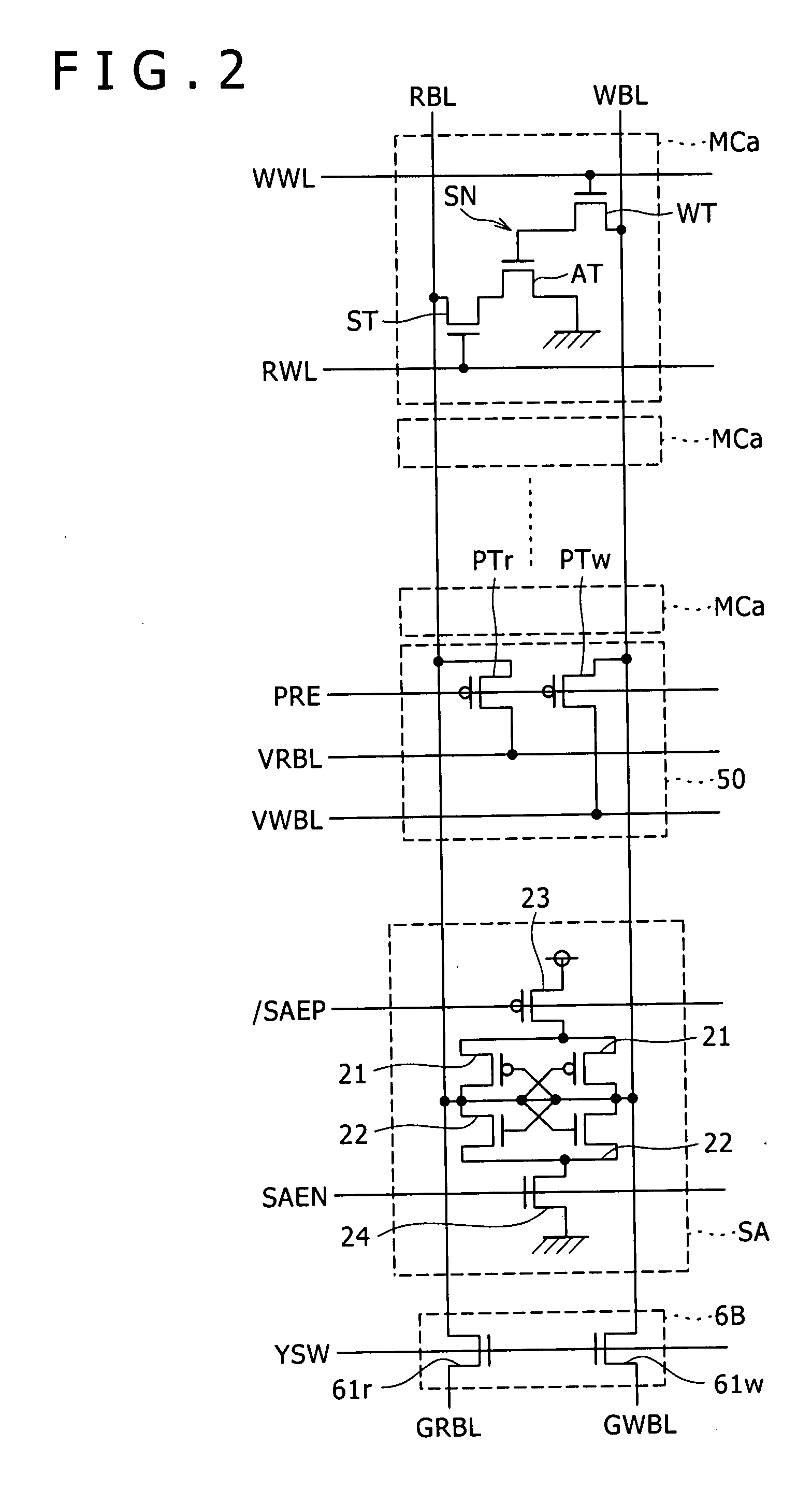
[0099]The semiconductor memory device shown in FIG. 8 has a memory cell array 1 having a number of memory cells MCa shown in FIG. 1 arranged in a matrix form and a peripheral circuit for the memory cell array 1.

[0100]The peripheral circuit includes an X-address decoder 2, a Y-address decoder 3, a row decoder 4, a column circuit 6, a BLI (Bit Line Isolation circuit) 8, an input / output (I / O) buffer 9, a WBL connection control circuit 10, and a control circuit 11.

[0101]One of the features of the semiconductor memory device is that the device has the BLI circuit 8 and the WBL connection control circuit 10. Details of the BLI circuit 8 and the WBL connection control circuit 10 are described hereinafter.

[0102]The X-address decoder 2 is a circuit for ...


PUM


Abstract

Disclosed herein is a semiconductor memory device including, a memory array with memory cells array-like arranged, a read bit line connected to a data output node of the memory cells and shared by a plurality of the memory cells arranged in one direction in the memory array, a write bit line connected to a data input node of the memory cells and shared by a plurality of the memory cells, a sense amplifier for sensing a voltage of the reading bit line, a first sense line and a second sense line connected to the sense amplifier, a read bit line switch for controlling electrical connection and disconnection between the first sense line and the read bit line, a write buffer connected between the second sense line and the write bit line, capable of controlling electrical connection and disconnection between the second sense line and the write bit line.

Description

CROSS REFERENCES TO RELATED APPLICATIONS[0001]The present invention contains subject matter related to Japanese Patent Application JP 2006-204800 filed in the Japan Patent Office on Jul. 27, 2006, the entire contents of which being incorporated herein by reference.BACKGROUND OF THE INVENTION[0002]1. Field of the Invention[0003]The present invention relates to a semiconductor memory device having a memory cell with a read bit line connected to a data output node thereof and also with a write bit line connected to a data input node thereof and enabling operations for reading and writing data via the pair of bit lines.[0004]2. Description of the Related Art[0005]There has been known the so-called gain cell as a memory cell with the data input node connected to a write bit line and the data output node connected to a read bit line.[0006]In the gain cell, there is provided an amplifier transistor that stores an electric charge in the so-called capacitive component added to a gate for dat...

Claims


Application Information

Patent Timeline
Patent Type & Authority Applications(United States)
IPC IPC(8): G11C11/409G11C5/14G11C7/00
CPCG11C7/067G11C7/12G11C7/18G11C8/10G11C8/12G11C2207/005G11C11/4087G11C11/4091G11C11/4094G11C11/4097G11C11/405
Inventor KITAGAWA, MAKOTO
Owner SONY CORP
Why Eureka
Try Eureka