Lighting Optical Device,Exposure System,And Exposure Method

a light optical device and exposure system technology, applied in the field of illumination optical apparatus, exposure apparatus, and exposure method, can solve the problems of failure to achieve the desired annular illumination, failure to achieve the desired small- circular illumination, and difficulty in avoiding the occurrence of zero-order light from the diffactive optical elemen

Inactive Publication Date: 2008-02-07
NIKON CORP
View PDF15 Cites 35 Cited by
  • Summary
  • Abstract
  • Description
  • Claims
  • Application Information

AI Technical Summary

Benefits of technology

[0038] preventing device disposed at a position where zero-order light from the diffractive optical element is focused, in an optical path of the shaping optical system, and adapted for preventing the zero-order light from the diffractive optical element from traveling along an illumination light path.

Problems solved by technology

It is, however, difficult to avoid occurrence of zero-order light from the diffractive optical element, for example, because of manufacture error or the like.
As a result, the unwanted surface illuminant is formed in the center of the annular secondary light source, which results in failure in accomplishment of desired annular illumination.
In the case of small-σ circular illumination using a relatively small, circular, secondary light source, however, an annular secondary light source substantially different from the desired circular shape is formed because of influence of the dark part, thus failing to accomplish the desired small-σ circular illumination.

Method used


Image

  • Lighting Optical Device,Exposure System,And Exposure Method
  • Lighting Optical Device,Exposure System,And Exposure Method
  • Lighting Optical Device,Exposure System,And Exposure Method

Examples


Embodiment Construction

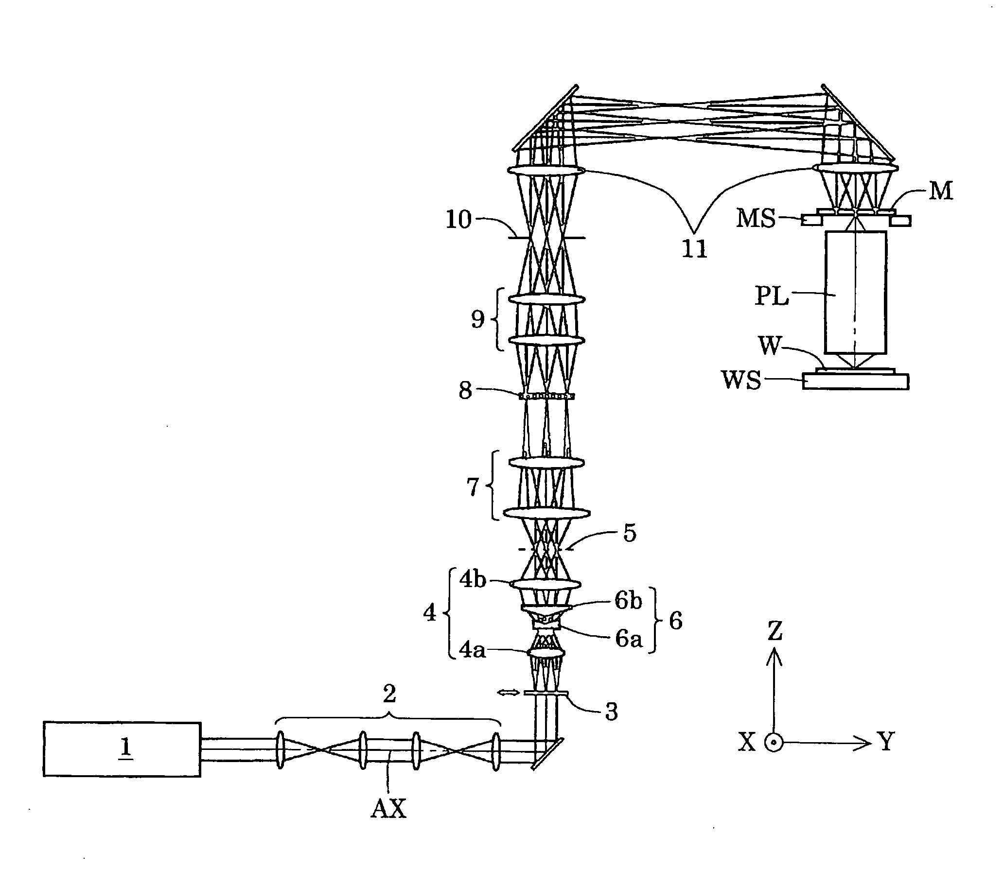
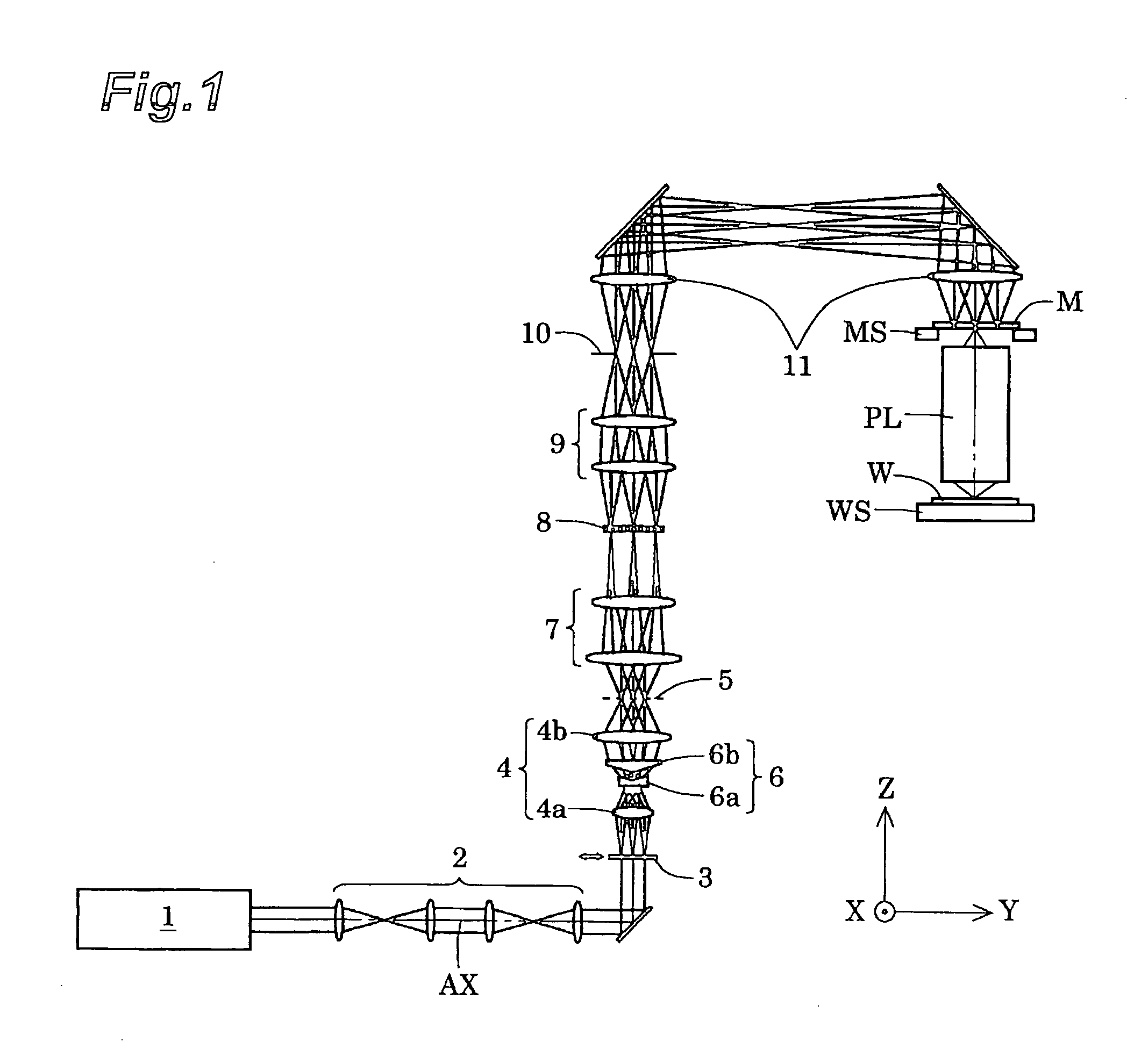
[0054] Embodiments of the present invention will be described on the basis of the accompanying drawings. FIG. 1 is a drawing schematically showing a configuration of an exposure apparatus according to an embodiment of the present invention. In FIG. 1, the Z-axis is set along a direction of a normal to a wafer W being a photosensitive substrate, the Y-axis along a direction parallel to the page of FIG. 1 in the surface of wafer W, and the X-axis along a direction perpendicular to the page of FIG. 1 in the surface of wafer W.

[0055] With reference to FIG. 1, the exposure apparatus of the present embodiment is provided with a light source 1 for supplying exposure light (illumination light). The light source 1 to be used can be, for example, an ArF excimer laser light source for supplying light of the wavelength of 193 nm. A nearly parallel light beam emitted from the light source 1 travels via a relay lens system 2 and a diffractive optical element 3 for annular illumination to enter a...


PUM


Abstract

An illumination optical apparatus is able to accomplish desired annular illumination, circular illumination, and so on, without substantial influence of the zero-order light from a diffractive optical element. The illumination optical apparatus comprises a diffractive optical element (3) which converts a light beam from a light source (1) into a light beam with a predetermined light intensity distribution; an optical integrator (8) disposed between the diffractive optical element and a surface to be illuminated (M) and adapted for forming a substantial surface illuminant on an illumination pupil plane on the basis of the light beam from the diffractive optical element; a shaping optical system (4, 6, 7) disposed between the diffractive optical element and the optical integrator and adapted for changing a size and shape of the substantial surface illuminant; and a preventing device disposed at a position substantially in the relation of Fourier transform with the diffractive optical element in an optical path of the shaping optical system, and adapted for preventing the zero-order light from the diffractive optical element from traveling along an illumination light path.

Description

CROSS-REFERENCE TO RELATED APPLICATIONS [0001] This application is based upon and claims the benefit of priorities from International Application No. PCT / JP2005 / 018809 filed on Oct. 12, 2005, and Japanese Patent Application No. 2004-110342 filed on Oct. 19, 2004, the entire contents of which are incorporated herein by reference. BACKGROUND [0002] 1. Field [0003] One embodiment of the present invention relates to an illumination optical apparatus, exposure apparatus, and exposure method and, more particularly, to an illumination optical apparatus suitably applicable to exposure apparatus for manufacturing micro devices, such as semiconductor devices, image pickup devices, liquid-crystal display devices, and thin-film magnetic heads, for example, by lithography. [0004] 2. Description of the Related Art [0005] In the typical exposure apparatus of this type, a light beam emitted from a light source is guided through a fly's eye lens as an optical integrator to form a secondary light sou...

Claims


Application Information

Patent Timeline
Patent Type & Authority Applications(United States)
IPC IPC(8): G02B15/00G02B27/42G02B27/46G02B3/02G02B7/00
CPCG02B5/001G02B27/46G03F7/70191G03F7/70108G03F7/70158G03F7/70075
Inventor SHIGEMATSU, KOJI
Owner NIKON CORP
Why Eureka
Try Eureka