Light emitters using nanotubes and methods of making same

a technology of nanotubes and light emitters, applied in the direction of discharge tubes/lamp details, nanoinformatics, discharge tube main electrodes, etc., can solve the problems of discrete components, inability to monolithically integrate, and typically micro-sized light emitters used in optoelectronic applications in the semiconductor industry. , to achieve the effect of low thermal conductivity and low thermal conductivity

Active Publication Date: 2008-02-14
NANTERO
View PDF99 Cites 25 Cited by
  • Summary
  • Abstract
  • Description
  • Claims
  • Application Information

AI Technical Summary

Benefits of technology

[0012]Under one aspect of the invention, a light emitter includes a nanotube article in electrical communication with a first and a second contact, a substrate having a predefined region with a relatively low thermal conductivity said region in predefined physical relation to said nanotube article; and a stimulus circuit in electrical communication wi...

Problems solved by technology

These devices are usually discrete, do not integrate with silicon, and usually emit a particular color, with multiple LEDs required to obtain a near-white light (in those applications where near-white ...

Method used


Image

  • Light emitters using nanotubes and methods of making same
  • Light emitters using nanotubes and methods of making same
  • Light emitters using nanotubes and methods of making same

Examples


example 1

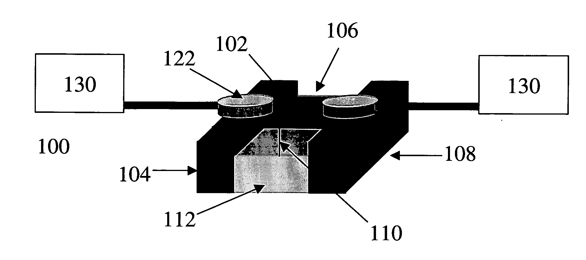
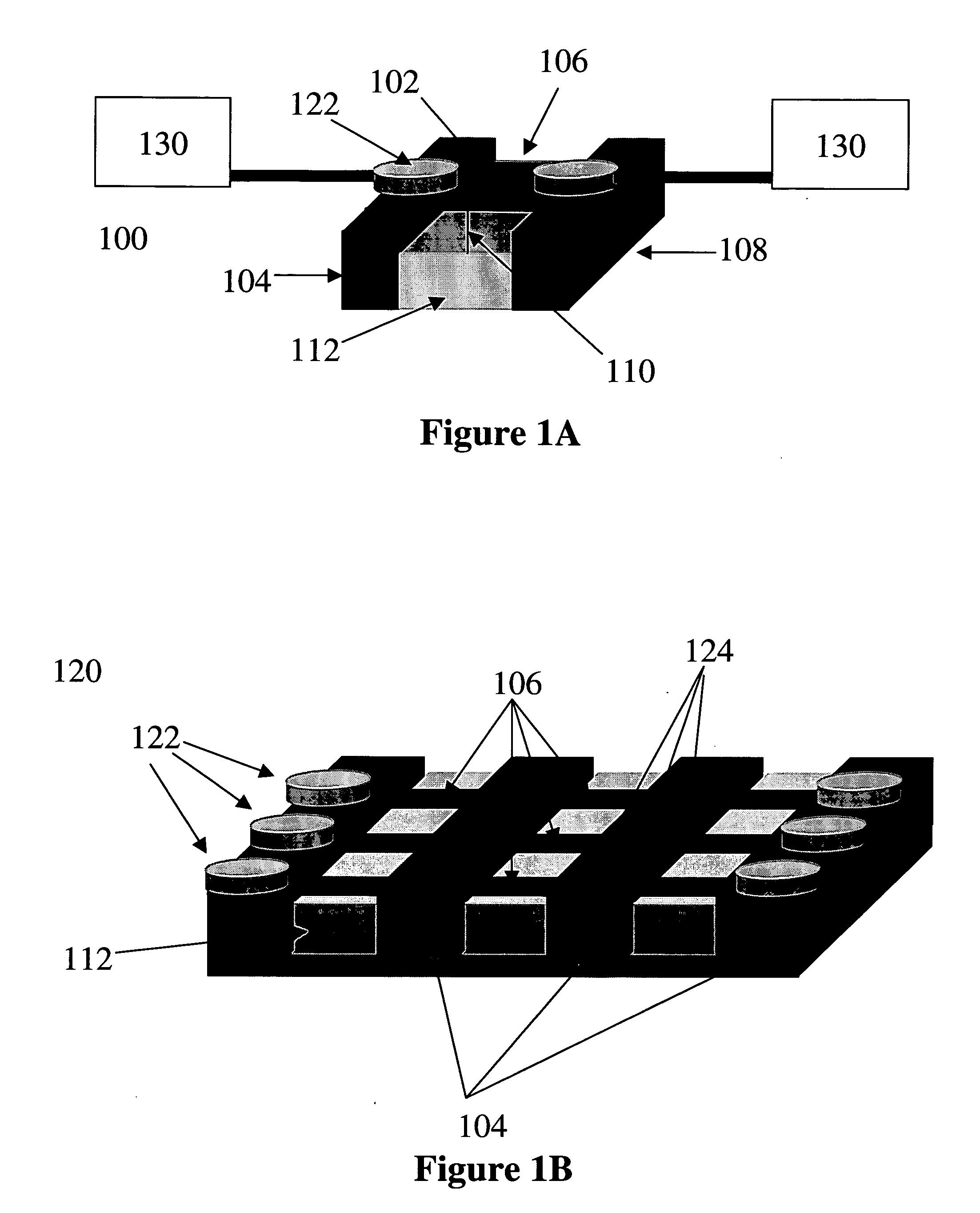
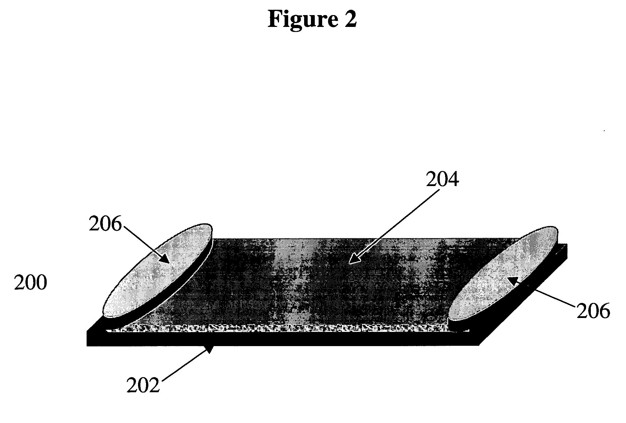
[0109]In this example, an addressable array of light emitting, suspended nanofabric articles is created. The setup is divided into three main parts:

[0110]the electrical control setup,

[0111]the chip holder; and

[0112]the optical detection setup.

[0113]The electrical control setup consists of a data acquisition system based on a National Instruments PCI-16XE-MIO-10 multipurpose DAQ card, with a BNC-2110 interface board. The DAQ card interface was written using National Instrument's Measurement Studio (Ver. 1.0) and Nidaq 7.01 with Microsoft's Visual Basic (Ver. 6.0). The electrical output (DAC0) goes through a Keithley 485 Pico-ammeter in order to measure the current going through the nanotube.

[0114]The electrical connections go through an interface connection with a sample holder (chip holder) designed to hold the 28 pin chips. The chip is has Argon gas flowing over the junction area (shown by the yellow tube going under the holder.

[0115]The optical detection setup consists of an Inver...


PUM


Abstract

Light emitters using nanotubes and methods of making same. A light emitter includes a nanotube article in electrical communication with a first and a second contact, a substrate having a predefined region with a relatively low thermal conductivity said region in predefined physical relation to said nanotube article; and a stimulus circuit in electrical communication with the first and second contacts. The stimulus circuit provides electrical stimulation sufficient to induce light emission from the nanotube article in the proximity of the predefined region. The predefined region is a channel formed in the substrate or a region of material with relatively low thermal conductivity. The light emitter can be integrated with semiconductor circuits including CMOS circuits. The light emitter can be integrated into optical driver circuits (on- and off-chip drivers) and opto-isolators.

Description

CROSS-REFERENCE TO RELATED APPLICATIONS [0001]This application claims priority under 35 U.S.C. §119(e) to U.S. Provisional Pat. Apl. No. 60 / 610,330, filed on Sep. 16, 2004, entitled Light Emitters Using Nanotubes and Methods of Making Same, which is incorporated herein by reference in its entirety.BACKGROUND [0002]1. Technical Field[0003]The present application relates generally to nanotube fabrics and methods of making same and, more specifically to carbon nanotube fabrics and methods of making same for use in light emitting systems.[0004]2. Discussion of Related Art[0005]Opto-electronics technologies have been utilized and developed in various fields such as the information input / output technologies and the optical communication technologies using optical fibers, and so on. Laser diodes have been developed as devices which support these opto-electronics technologies. For example, laser diodes can be used for reading compact discs and they can be used in optical communications.[000...

Claims


Application Information

Patent Timeline
IPC IPC(8): H01K1/02
CPCB82Y10/00B82Y20/00H01L51/0052H01L51/0048H01K1/04H10K85/221H10K85/615
Inventor WARD, JONATHAN W.MEINHOLD, MITCHELLBERTIN, CLAUDE L.SCHLATKA, BENJAMINSEGAL, BRENT M.RUCKES, THOMAS
Owner NANTERO
Why Eureka
Try Eureka