Switching Element, Switching Element Drive Method and Fabrication Method, Reconfigurable Logic Integrated Circuit, and Memory Element

Active Publication Date: 2008-02-14
NEC CORP
View PDF4 Cites 49 Cited by
  • Summary
  • Abstract
  • Description
  • Claims
  • Application Information

AI Technical Summary

Benefits of technology

[0017] In the present invention, the route of the metal interconnect depends on the route of the introduction path, and variation in the ON resistance between switching elements on the same wafer can be suppressed if the routes of the introduction paths are unified in each switching e

Problems solved by technology

As a result, the problem arises that variation occurs in the switching element ON resistance, which depends on the path of the metal interconnect, among switching elements existing on the same wafer.
This problem is believed to originate from differences in the locations where precipitate is prone to form in the surface of ion conduction layer that contacts the first electrode among switching elements that exist on the same wafer.
This type of variation in ON resistance greatly lowers the reliability of metal atom-mobile switching elements.
A further problem that arises in a two-terminal metal atom-mobile switching element such as described with reference to FIG. 1 is the low resist

Method used


Image

  • Switching Element, Switching Element Drive Method and Fabrication Method, Reconfigurable Logic Integrated Circuit, and Memory Element
  • Switching Element, Switching Element Drive Method and Fabrication Method, Reconfigurable Logic Integrated Circuit, and Memory Element
  • Switching Element, Switching Element Drive Method and Fabrication Method, Reconfigurable Logic Integrated Circuit, and Memory Element

Examples


first embodiment

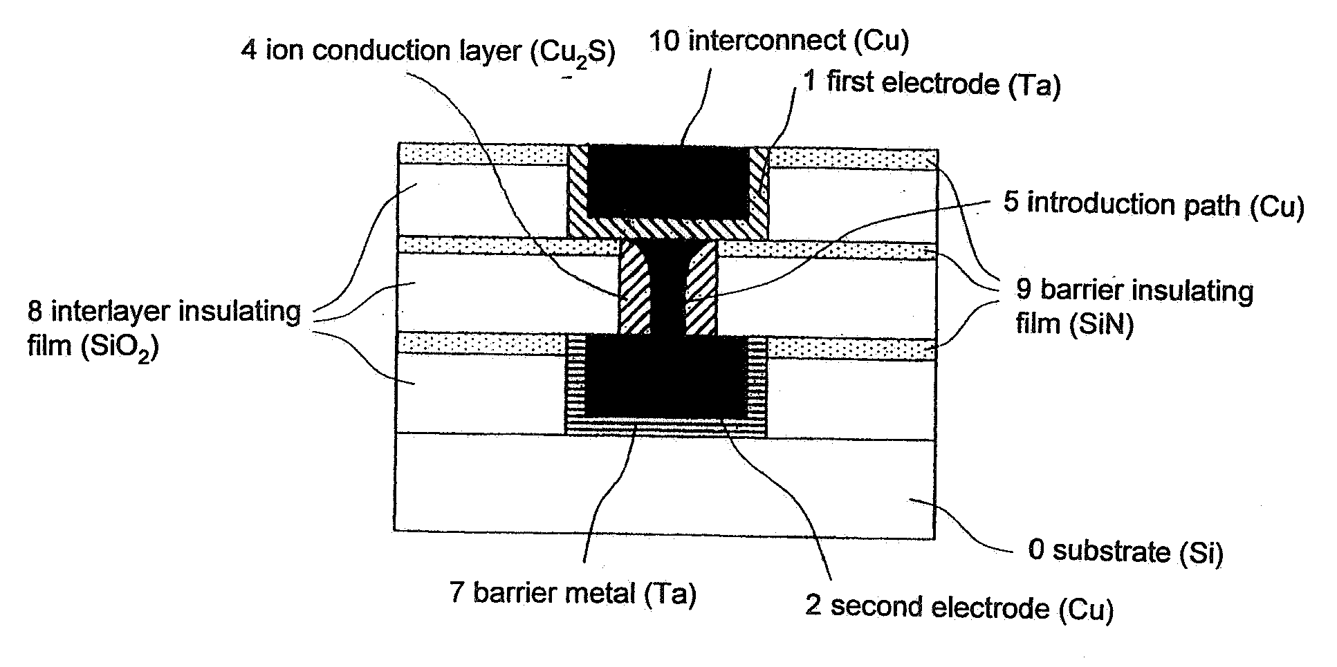
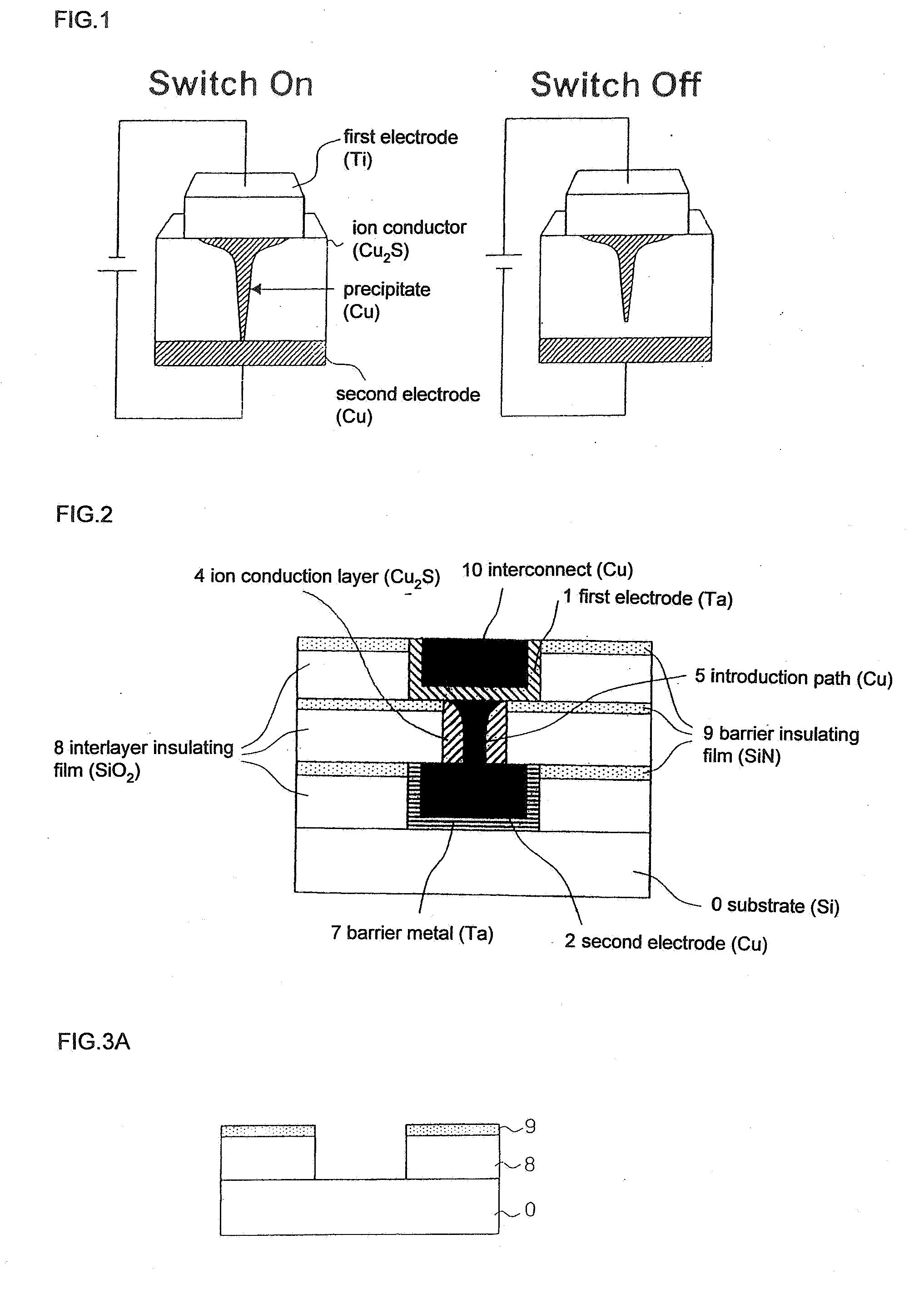
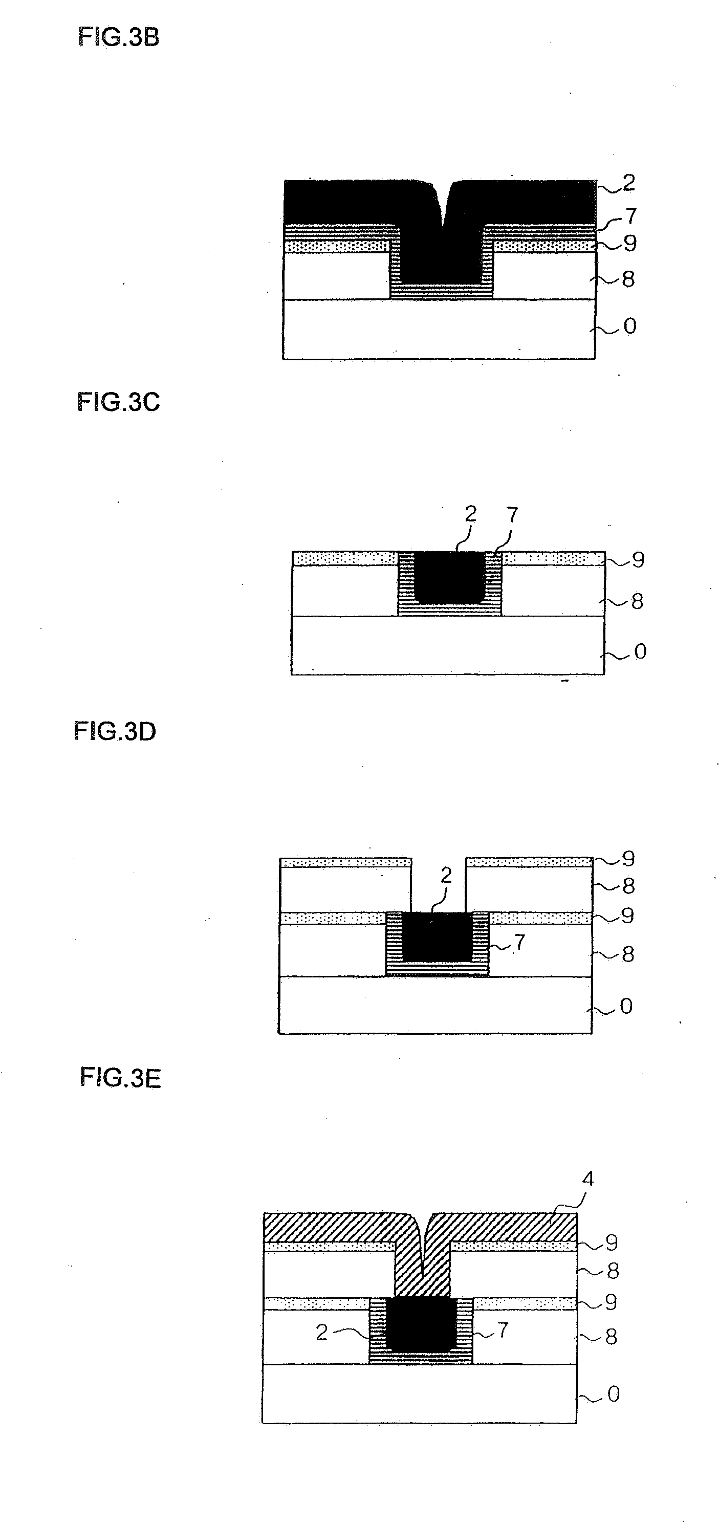
[0054] The metal atom-mobile switching element of the present embodiment is a device in which, compared to a conventional two-terminal metal atom-mobile switching element, the position of an introduction path for electrically connecting a first electrode and a second electrode is determined in advance in the design stage and in which the introduction path is formed in this position using the metal that makes up the second electrode in the fabrication stage. By thus providing the introduction path in a prescribed position in advance in the design stage and fabrication stage, the route of a metal interconnect that depends on the route of the introduction path is determined in the design stage and fabrication stage. By making this prescribed position common to all switching elements on the same wafer, the routes of the metal interconnects are common for all switching elements, whereby variation in the ON resistance among switching elements on the same wafer can be reduced. In addition,...

second embodiment

[0078] In the metal atom-mobile switching element of the present embodiment, the introduction path for electrically connecting the first electrode and second electrode is formed at a prescribed position in advance by a method that differs from the first embodiment. By thus forming the introduction path at a prescribed position in advance in the design stage and fabrication stage, the route of the metal interconnect that depends on the route of the introduction path is determined in the design stage and fabrication stage, enabling a reduction of the variation in the ON resistance among switching elements on the same wafer. In addition, the introduction path formed in advance in the design stage and fabrication stage is made sufficiently thick. Because the width of the metal interconnect depends on the width of the introduction path, the resistance against electromigration can be increased.

[0079] In addition, in the metal atom-mobile switching element of the present embodiment, a thi...

third embodiment

[0102] In the metal atom-mobile switching element of the second embodiment, introduction path 5 was formed in advance at a prescribed position between first electrode 1 and second electrode 2 in the design stage and fabrication stage, whereby the route of the metal interconnect was determined in the design stage and fabrication stage and variation in the ON resistance among switching elements on the same wafer was reduced. However, as an issue distinct from variation in the ON resistance, in a three-terminal metal atom-mobile switching element such as the metal atom-mobile switching element of the second embodiment, the metal interconnect composed of a precipitate is not formed between the first electrode and second electrode, but rather, is formed between the first electrode and third electrode, raising the concern of malfunctions of the switching element.

[0103] As a result, the route of the metal interconnect must be controlled in a three-terminal metal atom-mobile switching elem...


PUM


Abstract

The switching element of the present invention includes: an ion conduction layer (4) in which metal ions can move freely; a first electrode (1) that contacts the ion conduction layer (4); and a second electrode (2) that contacts the ion conduction layer (4), that is formed such that the ion conduction layer (4) is interposed between the first electrode (1) and the second electrode (2), and that supplies metal ions to the ion conduction layer (4) or that receives metal ions from the ion conduction layer (4) to cause precipitation of the metal that corresponds to the metal ions. An introduction path (5) composed of the metal and of a prescribed width is further provided on the ion conduction layer (4) for electrically connecting the first electrode (1) and the second electrode (2). The application of voltage to the first electrode (1) relative to the second electrode (2) then causes an electrochemical reaction between the introduction path (5) and the second electrode (2) whereby the electrical characteristics are switched.

Description

TECHNICAL FIELD [0001] The present invention relates to a switching element used in, for example, an integrated circuit, a drive method of the switching element, a fabrication method of the switching element, a reconfigurable logic integrated circuit that uses the switching element, and a memory element that uses the switching element. BACKGROUND ART [0002] A great quantity of integrated circuits are currently being used in electronic apparatuses. Many of the integrated circuits used in electronic apparatuses are Application-Specific Integrated Circuits (ASIC), and are dedicated circuits designed for specific electronic apparatuses. Among these application-specific integrated circuits, the arrangement of cells (logic circuits such as AND circuits and OR circuits) and connections between cells are carried out in the process of fabricating the integrated circuits and the circuit configuration therefore cannot be altered after fabrication. [0003] In recent years, competition in the dev...

Claims


Application Information

Patent Timeline
IPC IPC(8): H01L49/02
CPCH01L23/5252H01L27/2436H01L45/085H01L45/1206H01L45/1226H01L45/1233H01L45/1253H01L2924/0002H01L45/1266H01L45/142H01L45/1683H01L2924/00H10B63/30H10N70/253H10N70/245H10N70/823H10N70/8416H10N70/841H10N70/8822H10N70/066H10N70/826
Inventor SAKAMOTO, TOSHITSUGUKAWAURA, HISAO
Owner NEC CORP
Why Eureka
Try Eureka