Method of dry etching oxide semiconductor film

a technology of dry etching and oxide film, which is applied in the direction of semiconductor devices, decorative arts, photovoltaic energy generation, etc., can solve the problems of difficult to remove photoresist, low production yield, and high temperature melting and deformation of photoresist, and achieve high processing accuracy, high etch rate, and high processing accuracy

Inactive Publication Date: 2008-02-14
CANON KK
View PDF6 Cites 3966 Cited by
  • Summary
  • Abstract
  • Description
  • Claims
  • Application Information

AI Technical Summary

Benefits of technology

[0016]In order to solve the above-mentioned problems, the present invention provides a method of processing a film containing In—Ga—Zn—O with high processing accuracy. Further, the pres...

Problems solved by technology

However, the lift-off process as described above has a problem that a photoresist is melted and deformed at high temperature.
The lift-off process has another problem that when a photoresist is removed, an edge of a pattern of a deposited film is curved up, and thereafter an electric wire crossing over the pattern edge is liable to be broken, which lowers the production yield.
In this case, there arises a problem that a non-volatile substance is deposited on a surface of the photoresist after the etching, which makes it difficult to remove the photoresist even cleaned by an ultrasonic wave.
In principle, the etching proceeds isotropically in the wet etching, so that there arises a problem of genera...

Method used


Image

  • Method of dry etching oxide semiconductor film
  • Method of dry etching oxide semiconductor film
  • Method of dry etching oxide semiconductor film

Examples


examples

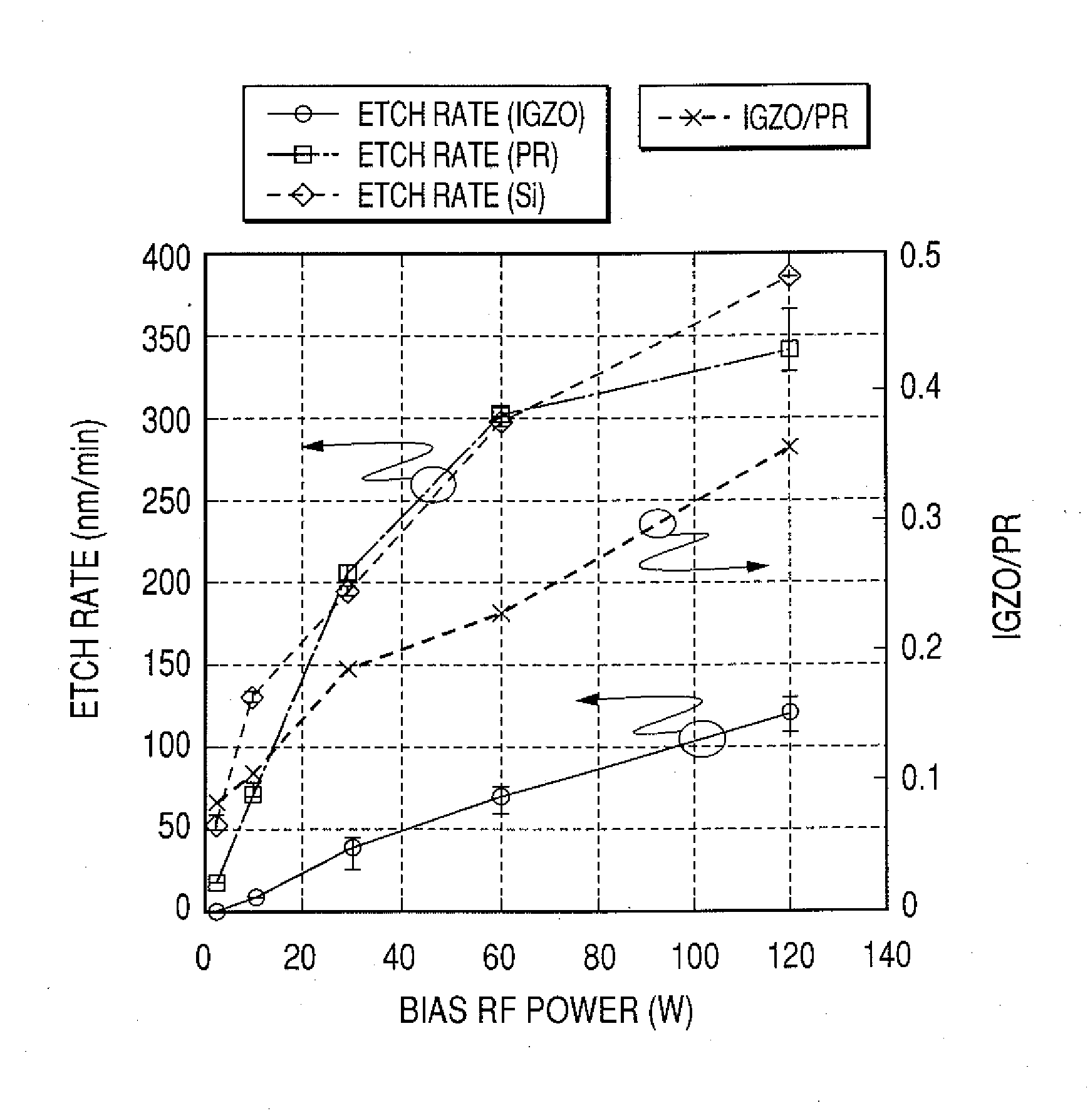
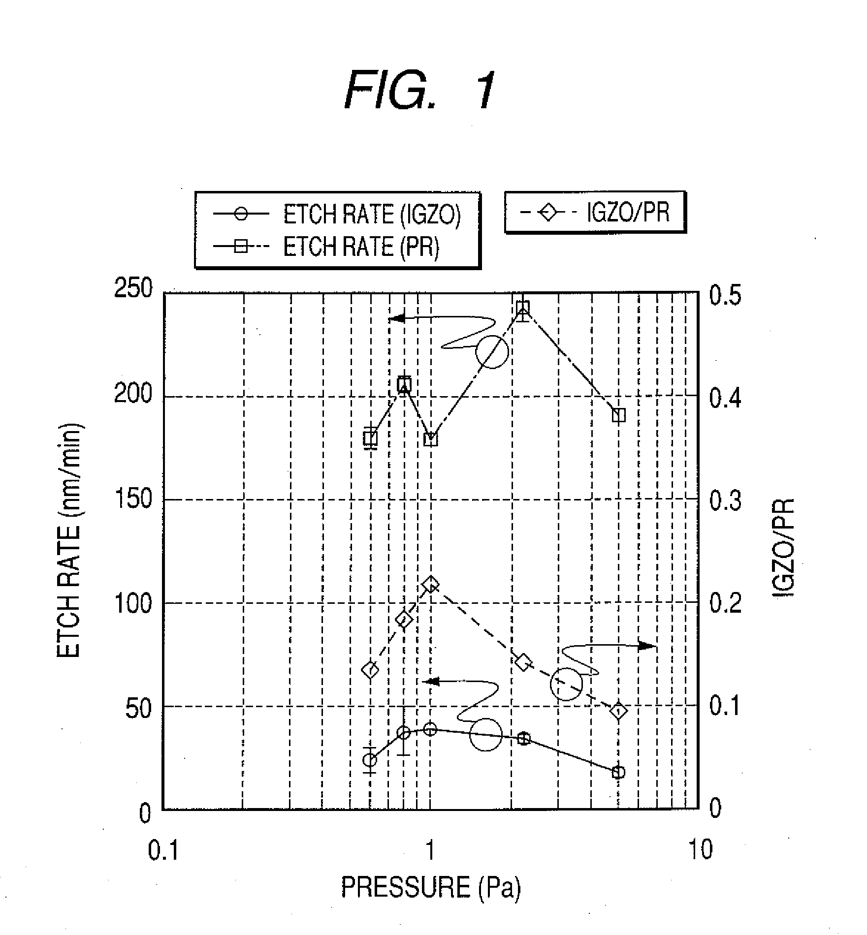
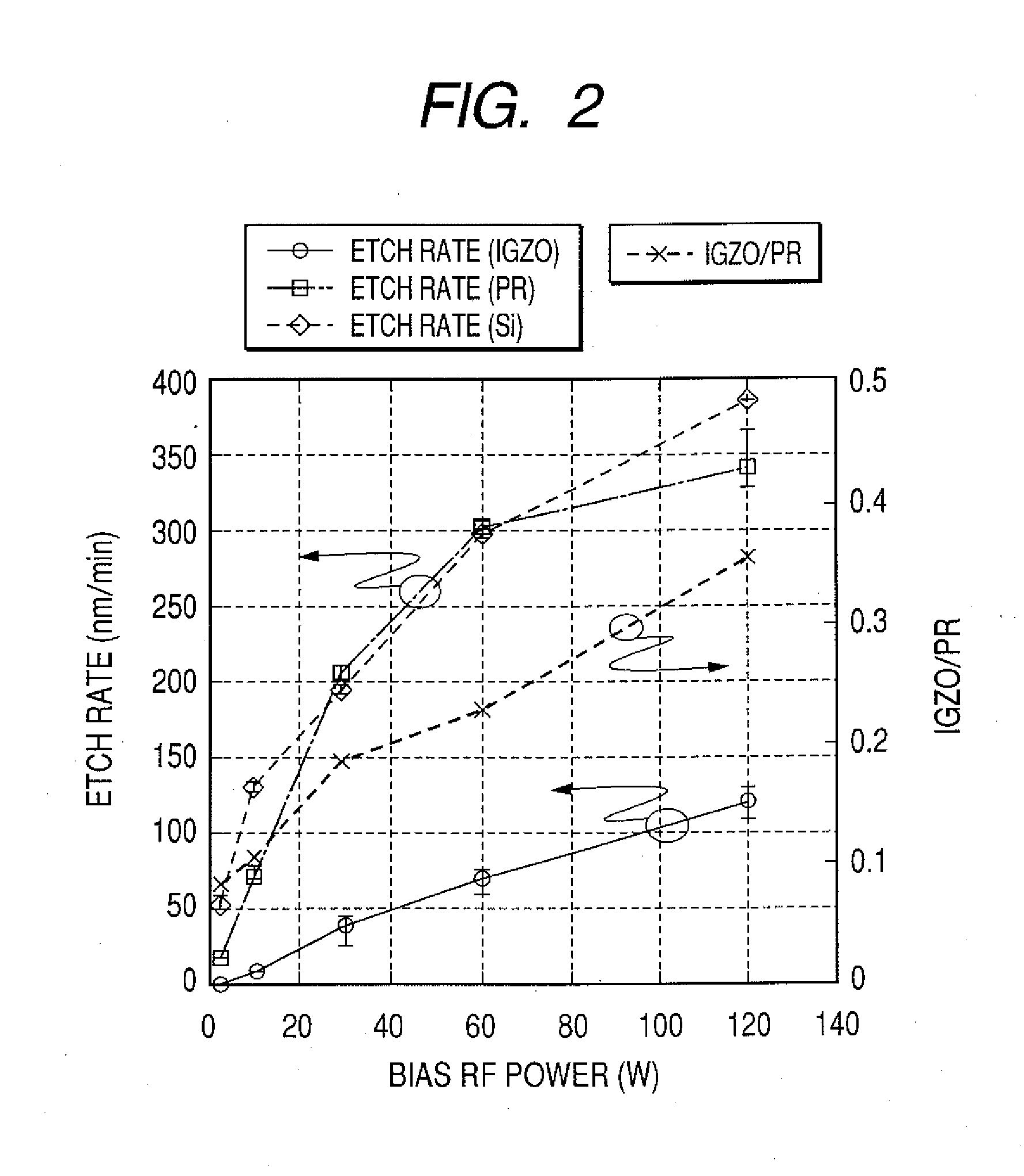
[0033]In the following description, specific examples of the dry etching method for the film containing In—Ga—Zn—O according to the present invention will be described. However, the present invention is not particularly limited to the examples.

[0034]First, a sample for an experiment was produced by a procedure described below. A Si substrate (thickness: 525 μm) having a Si oxide film with a thickness of 100 nm formed thereon was used as a base layer. Under the conditions as shown in Table 1, an In—Ga—Zn—O4 film having a thickness of 900 nm was formed by a reactive sputtering method.

TABLE 1TargetIn—Ga—Zn—O4SubstrateRoom TemperatureTemperature(60° C. or less)Ar flow rate50 sccmO2 flow rate0.6 sccmPressure0.326 PaRF power150 WTime40 minutesFilm Thickness900 nm

[0035]By the sputtering film forming method and by the use of a polycrystalline sintered body having an In—Ga—Zn—O4 composition as a target, an In—Ga—Zn—O-based amorphous oxide semiconductor thin film containing micro crystals was...


PUM

PropertyMeasurementUnit
Thicknessaaaaaaaaaa
Thicknessaaaaaaaaaa
Pressureaaaaaaaaaa

Abstract

Provided is a dry etching method for an oxide semiconductor film containing at least In, Ga, and Zn, which includes etching an oxide semiconductor film in a gas atmosphere containing a halogen-based gas.

Description

BACKGROUND OF THE INVENTION[0001]1. Field of the Invention[0002]The present invention relates to a method of dry etching an oxide film containing In, Ga, and Zn (hereinafter, referred to as “In—Ga—Zn—O”). In particular, the present invention relates to a method of dry etching an oxide semiconductor film containing In—Ga—Zn—O which is employed in producing a fine electronic component such as a semiconductor device, a semiconductor integration circuit, and an electrode.[0003]2. Description of the Related Art[0004]In recent years, as disclosed in Japanese Patent Application Laid-Open No. 2004-103957, research and development of a semiconductor oxide film containing In—Ga—Zn—O and its deposition conditions has been extensively conducted. Particularly because the semiconductor oxide film can be formed on a resin film at low temperature, its future application of the semiconductor oxide film to a portable electronic product with light weight has been targeted.[0005]Hitherto, the patternin...

Claims


Application Information

Patent Timeline
IPC IPC(8): H01L21/311
CPCH01L31/022466Y02E10/50H01L31/1884H01L31/022483
Inventor CHANG, CHIENLIU
Owner CANON KK
Why Eureka
Try Eureka