High sensitivity color filter array

a color filter array, high-sensitivity technology, applied in the field of electronic imaging sensors, can solve the problems of wasting available bandwidth considering the response characteristics of the human eye, affecting the s/n ratio, and the approach to color imaging has not been of practical significance until now, so as to achieve the effect of improving the s/n ratio

Active Publication Date: 2008-02-21
SAMSUNG ELECTRONICS CO LTD
View PDF15 Cites 16 Cited by
  • Summary
  • Abstract
  • Description
  • Claims
  • Application Information

AI Technical Summary

Benefits of technology

[0020]An imaging system formed according to the present invention includes the unique color filter arrangement of the present invention, and a standard image sensor, which provides an imaging system having an improved S / N ratio.

Problems solved by technology

A major problem with this approach is that the resulting signal presents the extracted color image information in a time order that is radically different from, for instance, standard NTSC or high definition ATSC video signals.
Finally, some of the color information (e.g., the blue image frame when a basic blue color filter is used) tends to be disproportionately detailed and hence wastes available bandwidth considering the response characteristics of the human eye.
In effect, elemental sample areas are defined along the filter stripes so that sampling for a given color is not uniform for both directions.
Such approaches to color imaging have not been of practical significance until now, however, in part because of the higher cost of fabricating the large number of individual elements required to produce adequate image detail.
Therefore, there is additional cost of fabricating a specific number of individual elements to provide sufficient image information and produce adequate detail.
However, the non-standard CFA configuration requires custom signal processing electronics, to recompose the raw color information into a suitable format; the coarse blue and red pixel distribution supplied by the so-called “de-mosaicing” electronics degrades chrominance resolution to a level below generally accepted standards.

Method used


Image

  • High sensitivity color filter array
  • High sensitivity color filter array
  • High sensitivity color filter array

Examples


Embodiment Construction

[0029]The following description is provided to enable any person skilled in the art to make and use the invention and sets forth the best modes contemplated by the inventor for carrying out the invention. Various modifications, however, will remain readily apparent to those skilled in the art. Any and all such modifications, equivalents and alternatives are intended to fall within the spirit and scope of the present invention.

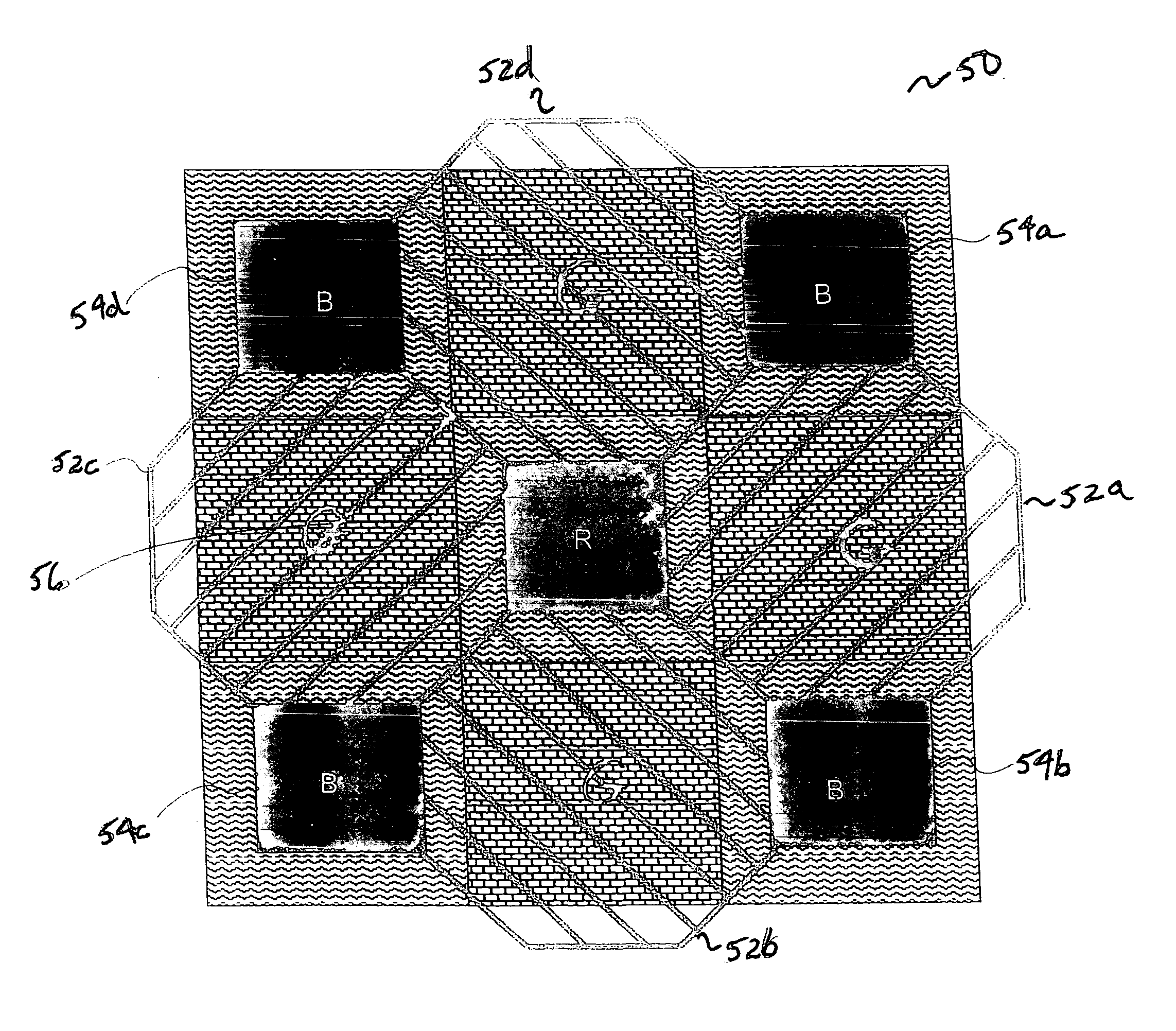
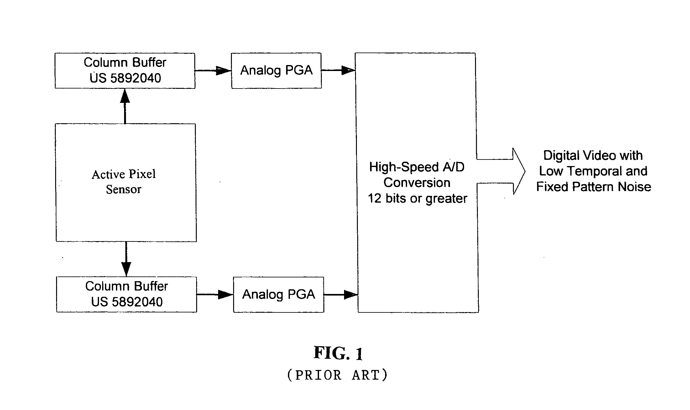
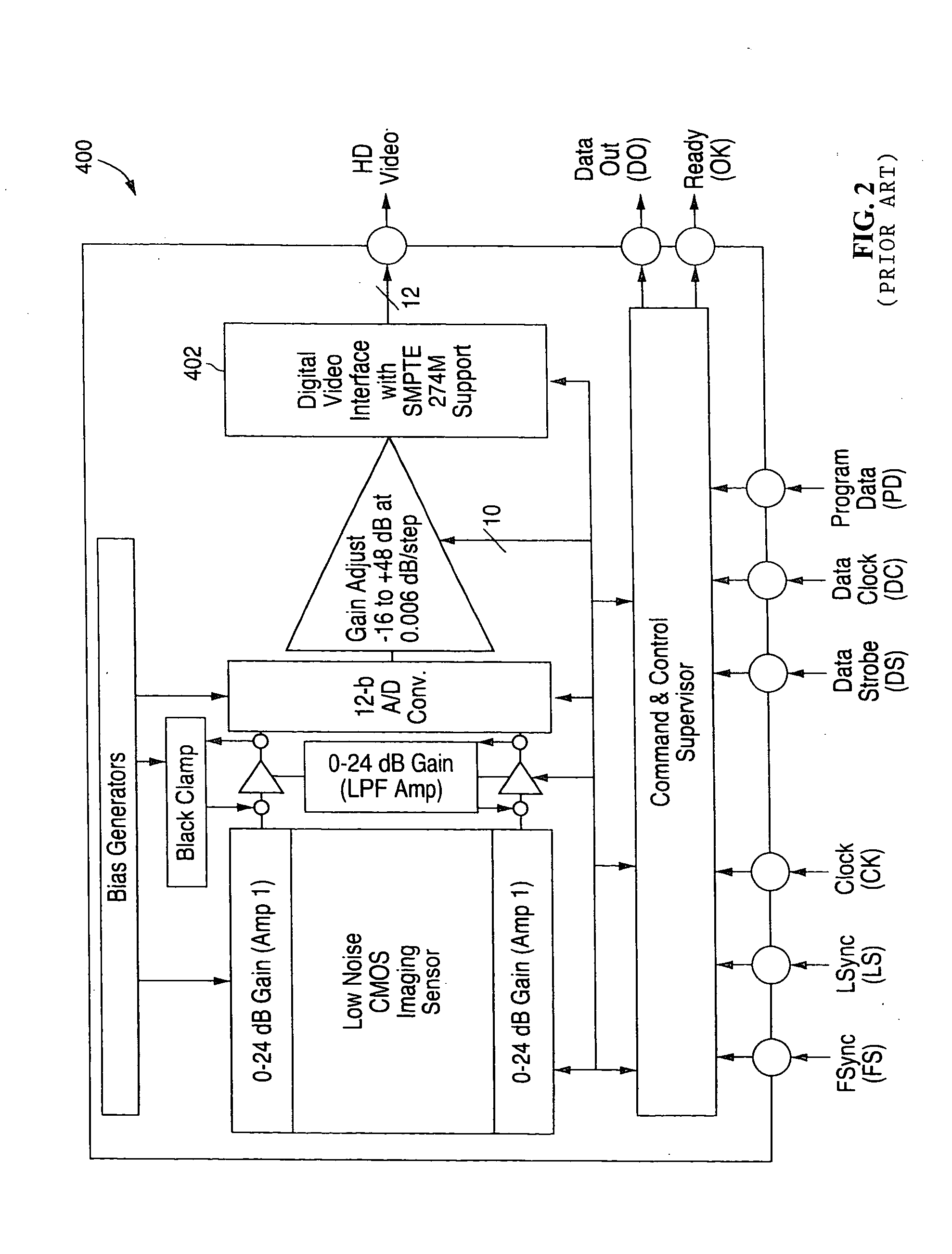
[0030]Visible imaging systems implemented in CMOS have the potential for significant reductions in cost and power requirements in components such as image sensors, drive electronics, and output signal conditioning electronics. A video camera, for example, can be configured as a single CMOS integrated circuit supported by only an oscillator and a battery. Such a CMOS imaging system requires lower voltages and dissipates less power than a CCD-based system. These improvements translate into smaller camera size, longer battery life, and applicability to many new pr...


PUM


Abstract

A color filter array (CFA) and image processing system wherein a color filter overlaying an image sensor has a luminance element (i.e. green filter in RGB space, or yellow in CMY space) that is made larger than the other two chrominance elements (i.e. red, blue or cyan, magenta). Additionally, overlaying micro-lenses may be sized to correspond to the relative sizes of the underlying color filters. The optimized filter array is compatible with existing de-mosaic image processing.

Description

BACKGROUND OF THE INVENTION[0001]1. Field of the Invention[0002]The present invention relates generally to electronic imaging sensors, and more particularly, to color filter arrays (CFAs) formed on the sensor to generate color images.[0003]2. Description of the Related Art[0004]Color cameras typically use charge-coupled-devices (CCD) or CMOS Image Sensors (CIS) to capture still images and generate live or recorded video. Although it is highly desirable to provide full color depth at each picture element (i.e., pixel) to minimize optical complexity and avoid problems with image registration in the spatial or temporal domains, cost and performance considerations often force each pixel to instead process a specific principal color. Full color images are subsequently formed by appropriately processing the color information from the entire color matrix. Various performance tradeoffs are encountered with such color matrices because at least three distinct types of color information must b...

Claims


Application Information

Patent Timeline
Patent Type & Authority Applications(United States)
IPC IPC(8): H04N9/04
CPCH01L27/14621H04N9/045H04N5/335H01L27/14627H04N25/00H04N25/134
Inventor KOZLOWSKI, LESTER J.
Owner SAMSUNG ELECTRONICS CO LTD
Why Eureka
Try Eureka