

Scan-type optical apparatus
- Summary
- Abstract
- Description
- Claims
- Application Information
AI Technical Summary
Benefits of technology
Problems solved by technology
Method used
Image

Examples
first embodiment
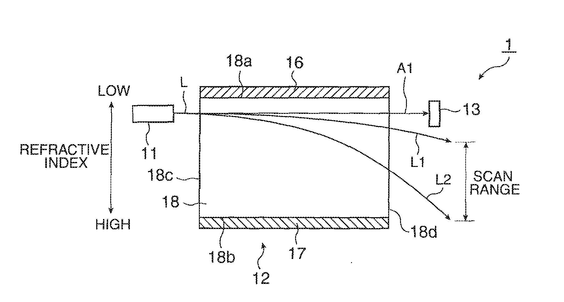
[0040]A scan-type optical apparatus 1 includes a light source device 11 for emitting laser beams, an electro-optic element 12 for conducting scan of the laser beams emitted from the light source device 11, a light blocking plate (light blocking member) 13 disposed on the light exit side of the electro-optical element 12.
[0041]As illustrated in FIG. 1A, the electro-optic element 12 has a first electrode 16, a second electrode 17, and an optical element 18.
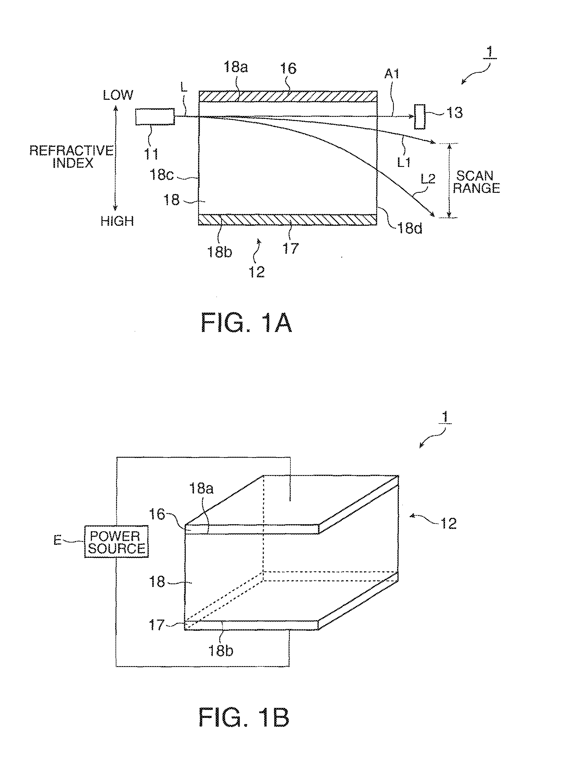
[0042]The optical element 18 is a dielectric crystal (electro-optic crystal) having electro-optic effect, and is constituted by a crystal material having a composition of KTN (potassium tantalate niobate; Kta1-xNbxO3) in this embodiment. As illustrated in FIG. 1B, the optical element 18 has a rectangular parallelepiped shape. The first electrode 16 is disposed on an upper surface 18a of the optical element 18, and the second electrode 17 is disposed on a lower surface 18b of the optical element 18. A power source E for applying volt...
second embodiment
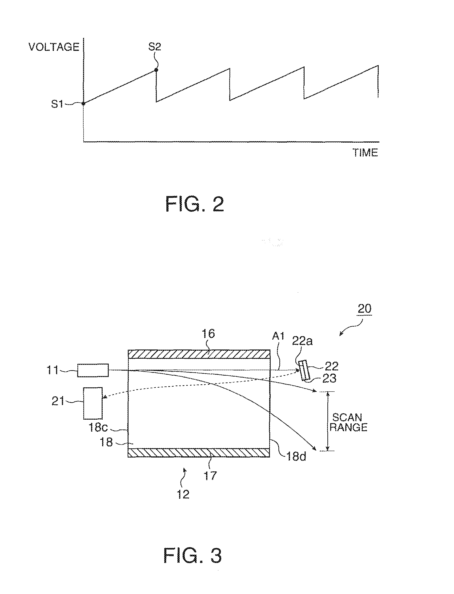
[0056]A second embodiment according to the invention is now described with reference to FIG. 3. In the following embodiments, similar reference numbers are given to the components and parts similar to those of the scan-type optical apparatus 1 in the first embodiment, and the same explanation of those is not repeated.
[0057]A scan-type optical apparatus 20 in this embodiment is different from the scan-type optical apparatus 1 in the first embodiment in that a light absorbing unit for absorbing laser beams at the stop of the electro-optic element is added.
[0058]A light blocking plate 22 has a reflection area 23 on a surface 22a opposed to the electro-optic element 12. The reflection area 23 is formed by a metal film having high reflectance. The reflection area 23 may be formed by a dielectric multilayer film.
[0059]The light blocking plate (light blocking member) 22 is disposed in such a position that the incident angle of the laser beam entering the reflection area 23 forms an angle w...
third embodiment
[0063]A third embodiment according to the invention is now described with reference to FIG. 4.
[0064]A scan-type optical apparatus 30 in this embodiment is different from the scan-type optical apparatus 1 in the first embodiment in that a mechanism for stopping emission of the laser beam when the electro-optic element stops is added.
[0065]A light blocking plate 31 has a photo diode (light detecting unit) 32 for executing photoelectric transfer on a surface 31a opposed to the electro-optic element 12.
[0066]The light source device 11 and the photo diode 32 are connected with a control unit 35. The control unit 35 controls the light source device 11 in accordance with the light detected by the photo diode 32. When the electro-optic element 12 fails for some reason, the laser beam emitted from the light source device 11 continuously irradiates the photo diode 32. Thus, the integral of energy detected by the photo diode 32 increases to a higher value than that when the electro-optic eleme...
PUM
 Abstract
Description
Claims
Application Information