Although conventional anti-fuses as described above have worked well in many applications, their use nevertheless may create several problems, particularly when used in more recent, high-density integrated circuits.
However, the magnitude of the programming voltage that can be applied to anti-fuses is severely limited by the presence of other circuitry in the
integrated circuit.
In particular, since the terminals on which the programming voltage is applied are typically used for other functions, excessive programming voltages can easily break down the
gate oxide layers of
MOSFET transistors connected to such terminal thereby making such transistors defective.
While this problem can be alleviated to some extent by increasing the
breakdown voltage of the bipolar ESD protection transistors, doing so may reduce the
safety margin of the ESD protection.
Furthermore, the problem would nevertheless remain because it would be difficult to isolate the programming voltage from the
integrated circuit substrate.
Failure to isolate the programming voltage from the substrate could cause excessive voltages to be coupled across the
gate oxide layers of
MOSFET transistors, even though the programming voltage was not applied directly to the gates of the transistors.
The problem of programming voltages breaking down the
gate oxide layer of
MOSFET's is exacerbated by the wide range of operating voltages of typical integrated circuits.
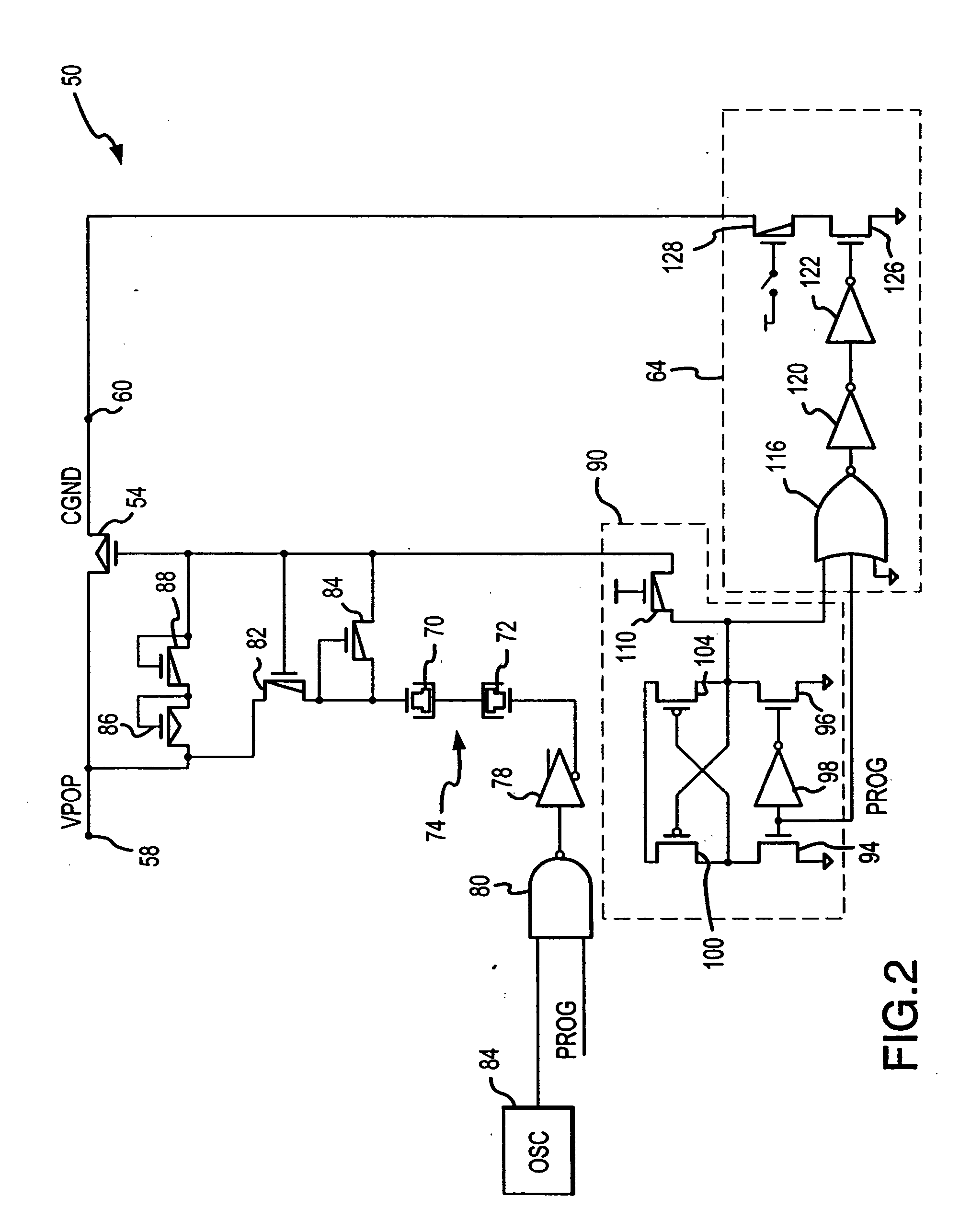
A significant limitation on the use of a bootstrap
capacitor is the limited duration in which the voltage applied to the gate of the isolation transistor remains above the programming voltage by at least the
threshold voltage VT.
However, as the charge on the
capacitor leaks away, both internally and through
external circuit components, the voltage applied to the gate of the isolation transistor decreases.
Thereafter, the isolation transistor can no longer couple the full magnitude of the programming voltage to the anti-fuse.
The time required to perform these multiple cycles can unduly increase the time required to program anti-fuses used in
semiconductor devices.
However, it has the
disadvantage of requiring a relatively large number of components in the charge pump, thereby increasing the cost of
semiconductor devices using this approach.
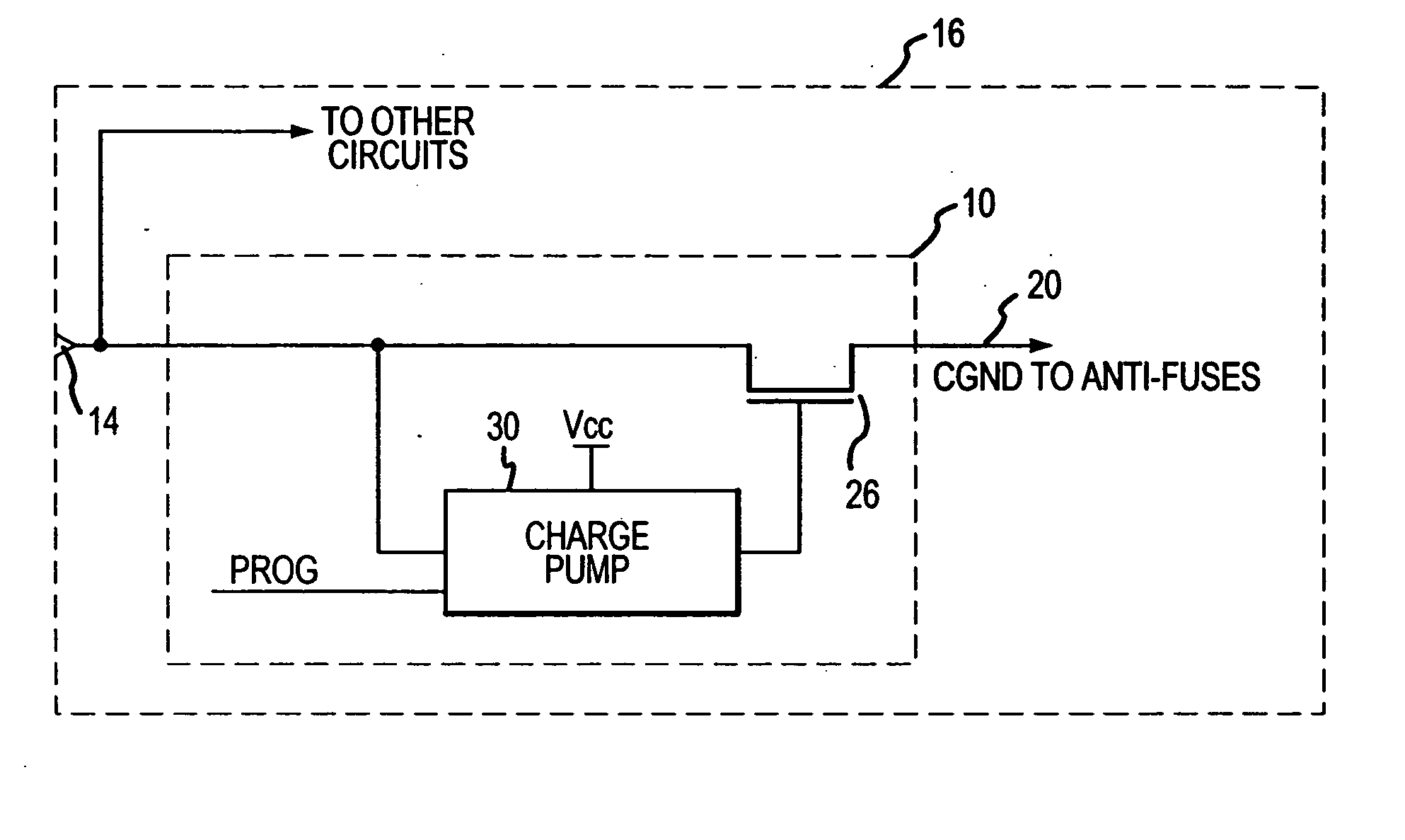
Although these conventional isolation circuits have been explained in the context of applying a positive programming voltage to an anti-fuse through an NMOS isolating transistor, it will be understood that the same or similar problem may exist when applying a negative programming voltage to an anti-fuse through a PMOS transistor.
Also, although the isolation circuits have been described as being coupled to an anti-fuse, it will be understood that the same or similar problem may exist when applying a programming voltage to other types of programmable elements, such as fuses.

