Methods of avoiding wafer breakage during manufacture of backside illuminated image sensors

Inactive Publication Date: 2008-02-21
TAIWAN SEMICON MFG CO LTD
View PDF13 Cites 113 Cited by
  • Summary
  • Abstract
  • Description
  • Claims
  • Application Information

AI Technical Summary

Benefits of technology

[0007]A method for processing a semiconductor device, comprising: providing a semiconductor wafer having a front side and a back side, the front side having circuit elements disposed thereon, said wafer further having a thickness, and a periphery having a bevel region; trimming

Problems solved by technology

Front-side illumination has significant performance limitations, however, such as low fill factor/low sensitivity, and limited spectral response, because the device's metal circuitry structure, which is formed on the front surface of the chip in the pixel region, obscures a portion of the pixel area, resulting in a loss of photons reaching the active area of the pixel.
Wafers can be broken very easily during this “thinning” process (or during handling), thus degrading wafer yields and making the ultimate CMOS BSI manufacturing processes (including manufacturing micro-lenses and color filters) commercially impractical.
The root cause of such breakage is believed to be the relatively poor

Method used


Image

  • Methods of avoiding wafer breakage during manufacture of backside illuminated image sensors
  • Methods of avoiding wafer breakage during manufacture of backside illuminated image sensors
  • Methods of avoiding wafer breakage during manufacture of backside illuminated image sensors

Examples


Embodiment Construction

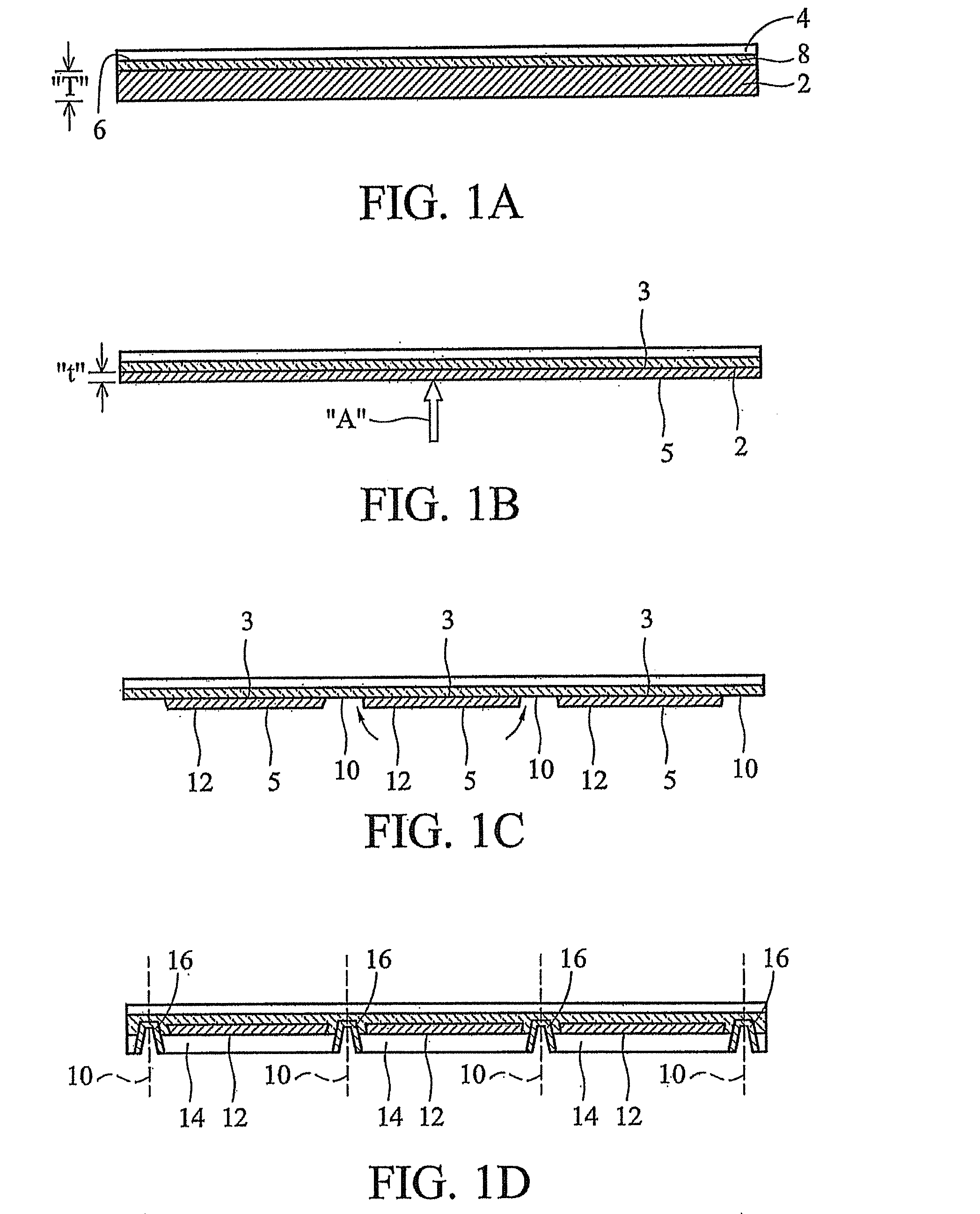
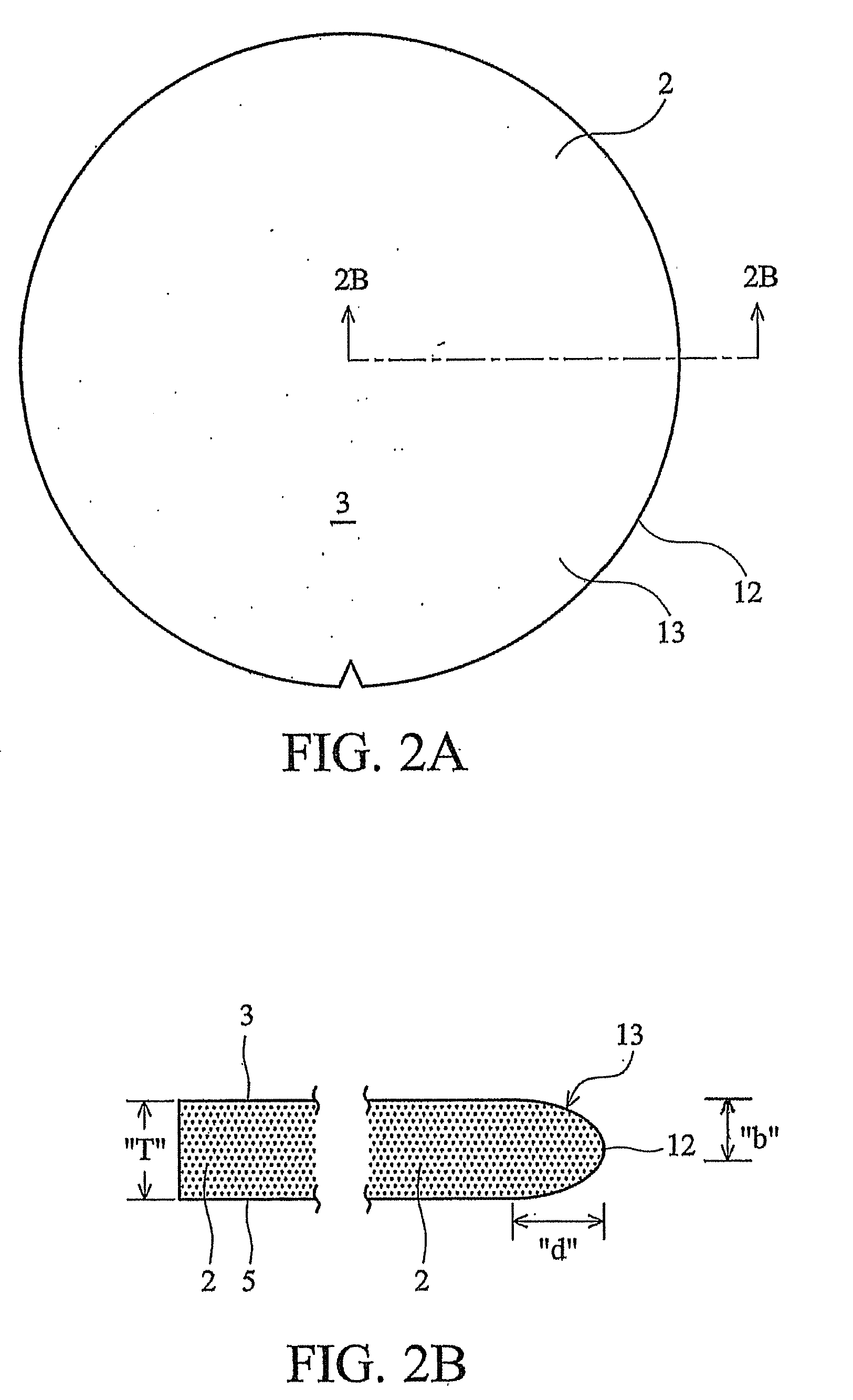
[0017]According to an embodiment of the present invention, disclosed herein is a method for reducing breakage of semiconductor wafers that presently occurs during the wafer thinning process associated with fabricating BSI CMOS devices. Specifically, a first example discloses trimming away a perimeter edge of the wafer prior to thinning the wafer. This trimming process may be implemented either before or after the wafer is bonded to a carrier substrate.

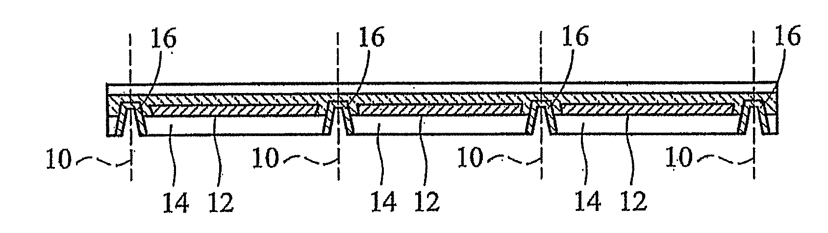
[0018]Referring to FIGS. 1A-D, an exemplary process for manufacturing a CMOS BSI imaging chip is shown. FIG. 1A shows a silicon wafer 2 bonded to a carrier substrate 4, which may be silicon, glass or other appropriate material. The wafer 2 may have a plurality of CMOS devices formed on one side, referred to as the “active surface”6. In the illustrated embodiment, the carrier substrate 4 is bonded to the wafer 2 such that the active surface 6 facing up toward the substrate 4. The carrier substrate 4 may be coated by an adhesive layer 8,...


PUM


Abstract

A process for forming backside illuminated devices is disclosed. Specifically, the process reduces processing damage to wafers caused by poor bond quality at the wafer edge ring. In one embodiment, a wafer edge trimming step is implemented prior to bonding the wafer to the substrate. A pre-grind blade is used to create a straight edge around the wafer perimeter, eliminating any sharp edges. In another embodiment, edge trimming is performed after the wafer has been bonded to the substrate, and a pre-grind blade is used to remove portion of the wafer edge ring subject to poor bonding quality before grinding. The final thickness of the ground wafer is about 50 microns in either case.

Description

FIELD OF THE INVENTION[0001]The present invention relates to a method for minimizing breakage of wafers during a wafer thinning process by trimming the beveled edge of the wafer prior to performing a wafer thinning process.BACKGROUND OF THE INVENTION[0002]Current complementary metal-oxide-semiconductor (CMOS) or charge coupled device (CCD) image sensors have traditionally employed front-side illumination for image pickup. Front-side illumination has significant performance limitations, however, such as low fill factor / low sensitivity, and limited spectral response, because the device's metal circuitry structure, which is formed on the front surface of the chip in the pixel region, obscures a portion of the pixel area, resulting in a loss of photons reaching the active area of the pixel.[0003]To solve these problems, especially for applications such as system-on-chip (SOC), four-transistor (4T) circuits, and for pixel sizes smaller than 1.7 micron×1.7 micron, back-side illuminated (B...

Claims


Application Information

Patent Timeline
IPC IPC(8): H01L21/30H01L21/46
CPCH01L21/304H01L27/14687H01L27/14618H01L2924/0002H01L2924/00
Inventor HSIEH, YUAN-CHIHYU, CHUNG-YISHIAU, GWO-YUHFU, SHIH-CHILIU, MING CHYITSAI, CHIA-SHIUNG
Owner TAIWAN SEMICON MFG CO LTD
Why Eureka
Try Eureka