Electronic components packaging structure

a technology for electronic components and packaging, applied in the field of packaging structures, can solve the problems of high cost, unstable performance of the resulting packaging structure, and components that are vulnerable to damage when touched, and achieve the effects of stable performance, reduced cost, and reduced possibility of malfunction

Active Publication Date: 2008-02-28
SHIMADZU CORP
View PDF6 Cites 18 Cited by
  • Summary
  • Abstract
  • Description
  • Claims
  • Application Information

AI Technical Summary

Benefits of technology

[0012]In the present invention, by housing at least one portion of the electronic component in the hole or the concave of the printed-circuit board, the surface of the printed-circuit board can be formed into a flat shape or a shape close to the flat shape. As a result, since the surface of the printed-circuit board is formed into the flat shape or the shape close to the flat shape, it becomes possible to package the component without applying a stress thereon, and consequently to provide stable performances. Even in the case of an electronic component that is vulnerable to malfunction when touched, since the possibility of touch is made smaller, the possibility of malfunction is also made smaller. Moreover, since one portion of the volume of the electronic component is received by the hole or the concave of the printed-circuit board, even a large-size component can be attached thereto. Since any of the above-mentioned structures can be achieved by using existing manufacturing line of electronic circuits and machining process, it is not necessary to prepare a new facility, thereby making it possible to reduce the costs.

Problems solved by technology

Here, since electronic components such as sensors mounted on the substrate surface can be easily touched, those components that are vulnerable to damage when touched tend to have a higher possibility of malfunction.
The substrate surface is not flat when electronic components have been mounted thereon; therefore, in the case when a component that is adversely affected in its performances upon receipt of a stress is mounted, it is highly possible that the performances of the resulting packaging structure become unstable.
Moreover, upon packaging a substrate on which electronic components have been mounted on a pipe-shaped member having a limitation in its space, those components having a large volume are not adopted in some cases.
As a result, instead of using an inexpensive component having a large volume, a component that has a smaller volume, but is expensive, needs to be mounted to sometimes cause high costs.

Method used


Image

  • Electronic components packaging structure
  • Electronic components packaging structure
  • Electronic components packaging structure

Examples


embodiment 1

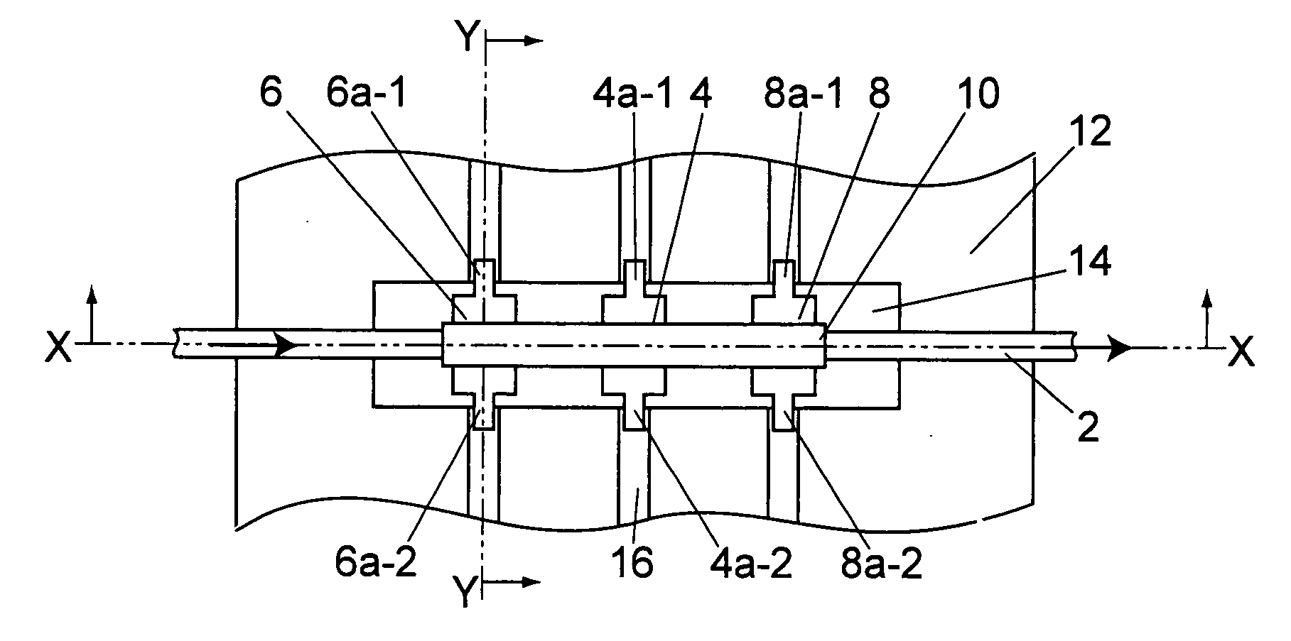
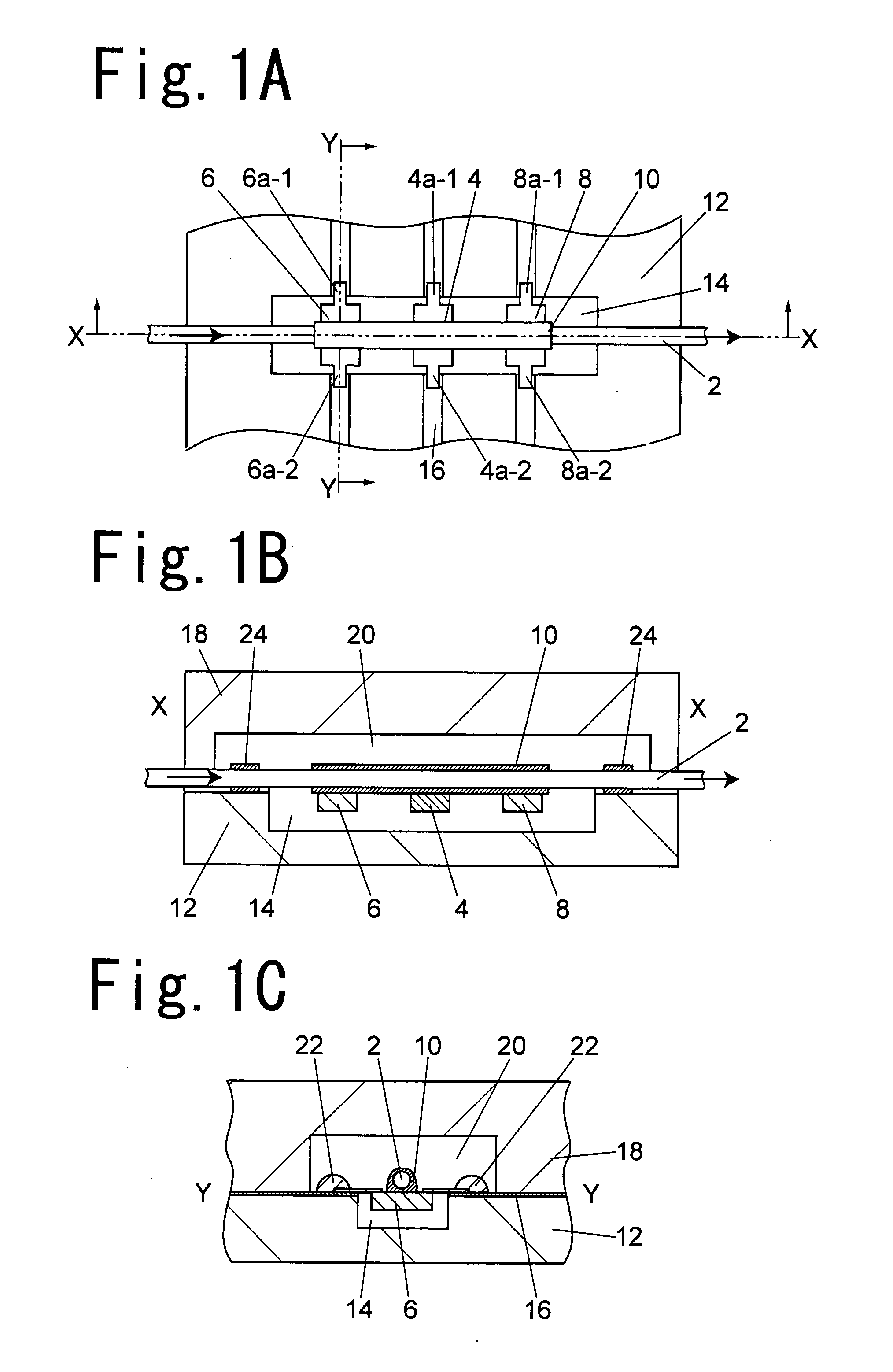
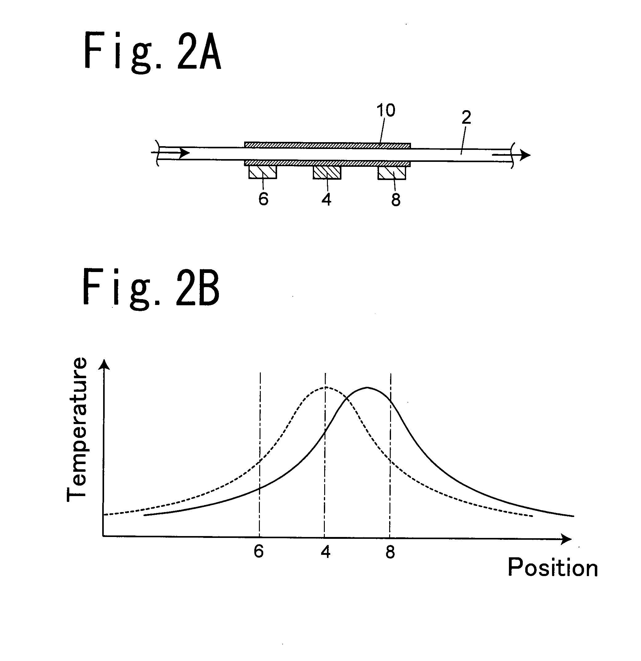
[0031]The following description will discuss a thermal mass flow meter utilizing chip diodes as a first embodiment FIG. 1A is a plan view that shows one embodiment of a thermal mass flow meter, FIG. 1B is a cross-sectional view at X-X position of FIG. 1A, and FIG. 1C is a cross-sectional view at Y-Y position of FIG. 1A. In this embodiment, a cover 18 used for covering a measuring unit of the thermal mass flow meter from above is provided; however, this is not shown in FIG. 1A.

[0032]A pipe arrangement 2 is placed on a horizontal face, and one of the faces of the pipe arrangement 2 is referred to as upper side, and the other face thereof is referred to as lower side. Moreover, in this embodiment, the pipe arrangement 2 is placed on the horizontal face, and this embodiment also includes structures in which the pipe arrangement 2 is placed in a vertical direction or in a tilted state, and in these cases also, one of the faces thereof is referred to as upper side, and the other face ther...

embodiment 2

[0052]Referring to FIGS. 3A to 3C, the following description will discuss an example in which the electronic component packaging structure of the present invention is applied to a thermal current meter as a second embodiment FIG. 3A is a plan view, FIG. 3B is a cross-sectional view taken along a metal thin wire, and FIG. 3C is a side view.

[0053]A hole 32 is formed in a printed-circuit board 30, and a metal thin line 34 is housed in the hole 32. One end of the metal thin wire 34 is solder-connected to a contact pad 36 that is connected to a wiring layer on the surface side of the printed-circuit board 30, with the other end being solder-connected to a contact pad 38 that is connected to a wiring layer on the rear face side of the printed-circuit board 30. With this arrangement, the metal thin wire 34 is electrically connected to the printed-circuit board 30, and is also mechanically secured thereto.

[0054]The thermal current meter has a structure in which a constant electric current i...

embodiment 3

[0058]The following description will discuss an example in which the electronic component packaging structure of the present invention is applied to a Pirani gauge. The Pirani gauge has basically the same operational principle as the thermal current meter. It has a structure in which a constant current is allowed to flow through a metal thin wire to be heated so that the fact that the electrical resistance of the metal thin wire is changed by the temperature is utilized. The thermal conductivity varies depending on the degree of vacuum to cause a change in the temperature of the metal thin wire. The change in resistance of the metal thin wire is read so that the correlation between it and the degree of vacuum is acquired.

[0059]In the Pirani gauge to which the present invention is applied also, the same effects as explained in the thermal current meter of embodiment 2 can be obtained.


PUM


Abstract

In a preferred embodiment, a thermal mass flow meter is provided with: a pipe arrangement that allows a fluid to flow therein, a chip-type heat-generating element that is anchored on the surface on the periphery of the pipe arrangement and used for heating the fluid in the pipe arrangement, and paired chip-type temperature sensors that are anchored at positions on the upstream side and the downstream side of the heat-generating element with the same distance apart therefrom, on the surface of the pipe arrangement, and formed as members separated from the heat-generating element. With respect to the heat-generating element and the paired temperature sensors, convex portions thereof on a side opposite to the side to be anchored onto the pipe arrangement are housed in a concave of a printed-circuit board, and terminals of the heat-generating element and the paired temperature sensors are connected to the wiring layer of the printed-circuit board, and subsequently secured to the printed-circuit board.

Description

BACKGROUND OF THE INVENTION[0001]1. Field of the Invention[0002]This invention relates to a packaging structure in which electronic components are mounted on a substrate. With respect to such a packaging structure, for example, thermal mass flow meters, thermal current meters, Pirani gauges, light-emitting element packaging structures and packaging structures of an electronic component such as a large-capacity capacitor are listed.[0003]2. Description of the Related Art[0004]Upon packaging an electronic componet such as a sensor on a substrate such as a printed-circuit board, normally, the electronic component is mounted on the surface of the substrate. For this reason, the substrate of the packaging structure comes to have a surface with irregularities.[0005]For example, as a thermal flow sensor used for measuring a flow speed or a flow rate of a fluid, such a flow sensor has been known in which a heat-generating resistor forming a flow-speed detecting resistance and a temperature ...

Claims


Application Information

Patent Timeline
Patent Type & Authority Applications(United States)
IPC IPC(8): G01F1/69G01F1/688H05K1/02H05K1/16
CPCG01F1/684G01F1/6847G01F1/688H05K2201/10151H05K1/182H05K2201/10015H05K2201/10106G01F1/6888
Inventor HASEBE, SHINYA
Owner SHIMADZU CORP
Why Eureka
Try Eureka