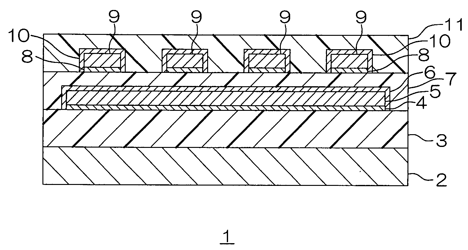
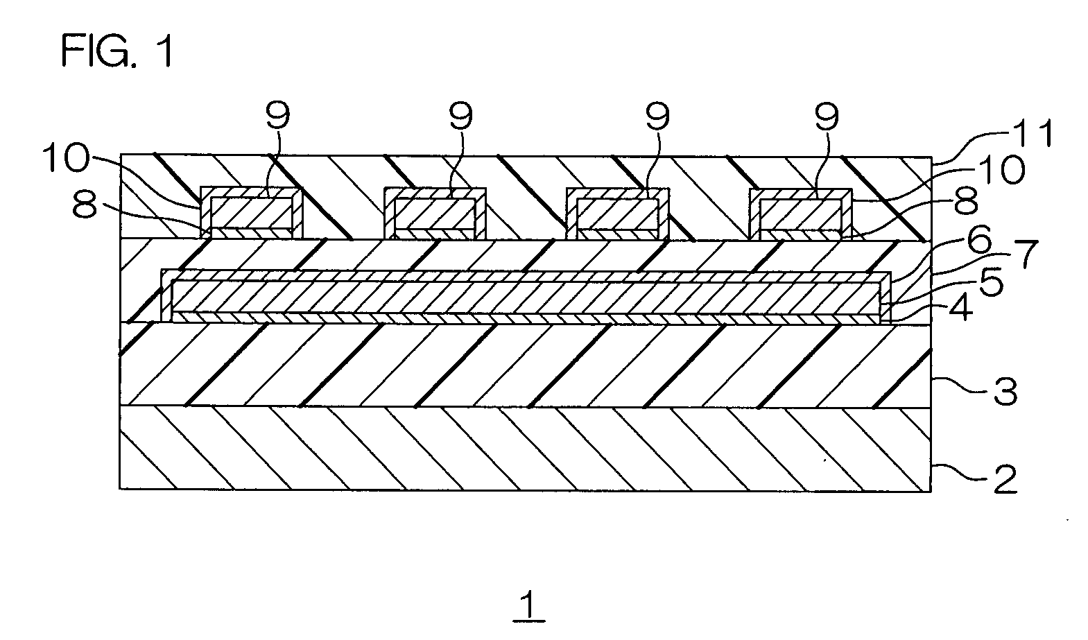
Wired circuit board

a wired circuit board and circuit board technology, applied in the direction of printed circuit aspects, high frequency circuit adaptations, cross-talk/noise/interference reduction, etc., can solve the problems of difficult to ensure long-term reliability, insufficient adhesion between the insulating layer and the lower conductor, etc., to improve adhesion, reduce transmission loss, simple layer structure

Inactive Publication Date: 2008-02-28
NITTO DENKO CORP
View PDF19 Cites 11 Cited by
  • Summary
  • Abstract
  • Description
  • Claims
  • Application Information

AI Technical Summary

Benefits of technology

[0010]In the wired circuit board according to the present invention, the metal foil is formed under the conductive pattern. This allows a reduction in transmission loss with a simple layer structure. In addition, the first metal thin film is formed between the first insulating layer and the metal foil. This makes it possible to sufficiently improve the adhesion between the first insulating layer and the metal foil and ensure excellent long-term reliability.

Problems solved by technology

However, in accordance with the proposal mentioned above, the adhesion between the insulating layer and the lower conductor is insufficient and it is difficult to ensure long-term reliability.

Method used


Image

  • Wired circuit board
  • Wired circuit board
  • Wired circuit board

Examples


example 1

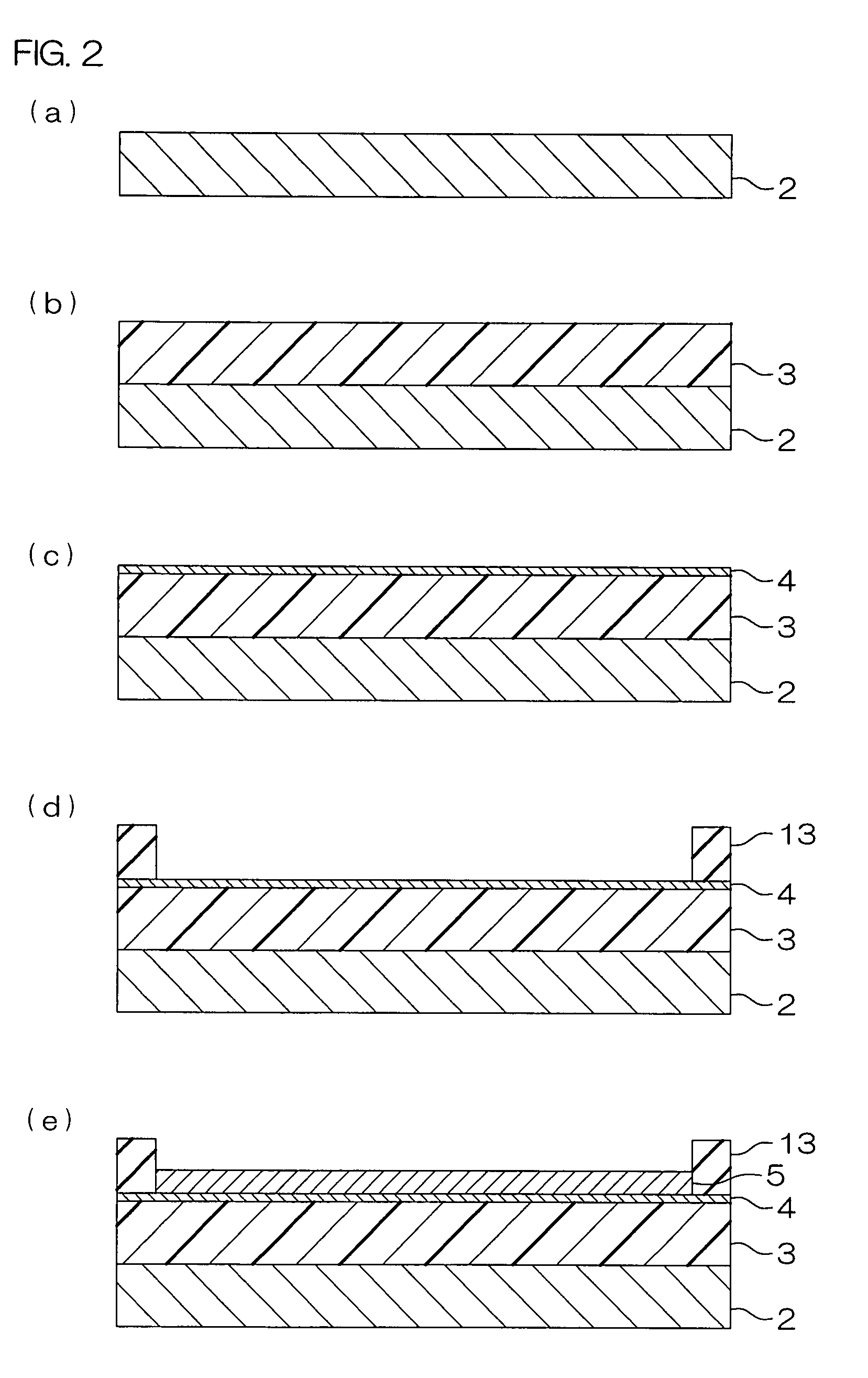
[0076]A metal supporting board made of stainless steel having a thickness of 25 μm was prepared first (see FIG. 2(a)). A varnish of a photosensitive polyamic acid resin was coated on the surface of the metal supporting board, dried, exposed to light, developed, and further heated to be cured to form a first insulating base layer made of polyimide having a thickness of 10 μm in the foregoing pattern (see FIG. 2(b)).

[0077]Then, a chromium thin film having a thickness of 0.03 μm and a copper thin film having a thickness of 0.07 μm were successively laminated on the entire surface of the first insulating base layer by chromium sputtering and copper sputtering to form a first metal thin film (see FIG. 2(c)). Then, a plating resist was formed in the foregoing pattern reverse to the pattern of a metal foil by providing a dry film resist on the surface of the first metal thin film, exposing it to light, and developing it (see FIG. 2(d)). Subsequently, a copper foil having a thickness of 4.0...

example 2

[0084]A suspension board with circuit was obtained in the same manner as in EXAMPLE 1 except that the second insulating base layer was formed on the first insulating base layer to cover the upper surface and both widthwise side surfaces of the metal foil and both the widthwise side surfaces of the first metal thin film without forming the second metal thin film.

Comparitive Example 1

[0085]A suspension board with circuit was obtained in the same manner as in EXAMPLE 1 except that the metal foil was formed directly on the surface of the first insulating base layer without forming the first metal thin film.

[0086]The metal foil was formed by a subtractive method, more specifically, by sticking a metal layer to the entire surface of the first insulating base layer via an adhesive layer, providing a dry film resist on the surface of the metal layer, exposing it to light, and developing it to form an etching resist in the same pattern as that of the metal foil, performing wet etching with r...


PUM

PropertyMeasurementUnit
thicknessaaaaaaaaaa
thicknessaaaaaaaaaa
thicknessaaaaaaaaaa

Abstract

A wired circuit board has a metal supporting board, a first insulating layer formed on the metal supporting board, a first metal thin film formed on the first insulating layer, a metal foil formed on the first metal thin film, a second insulating layer formed on the first insulating layer to cover the metal foil, and a conductive pattern formed on the second insulating layer.

Description

CROSS-REFERENCE TO RELATED APPLICATION[0001]This patent application claims the benefit of U.S. Provisional Application No. 60 / 847,111, filed on Sep. 26, 2006, and claims priority from Japanese Patent Application No. 2006-206642, filed on Jul. 28, 2006, the contents of which are herein incorporated by reference in their entirety.FIELD OF THE INVENTION[0002]The present invention relates to a wired circuit board and, more particularly, to a wired circuit board such as a suspension board with circuit.DESCRIPTION OF THE RELATED ART[0003]There has been conventionally known a suspension board with circuit in which an insulating layer made of a resin and a conductive pattern made of copper are formed successively on a metal supporting board made of stainless steel.[0004]In such a suspension board with circuit, a transmission loss is large in a conductive pattern since the metal supporting board is made of stainless steel.[0005]To reduce the transmission loss, it is proposed that, e.g., a lo...

Claims


Application Information

Patent Timeline
Patent Type & Authority Applications(United States)
IPC IPC(8): H05K1/05
CPCH05K1/0218H05K1/0237H05K1/056H05K2201/0723H05K3/181H05K3/388H05K3/4644H05K3/108
Inventor ISHII, JUNYOKAI, TAKAHIKO
Owner NITTO DENKO CORP
Why Eureka
Try Eureka