

Semiconductor device manufacturing method, data generating apparatus, data generating method and recording medium readable by computer recoded with data generating program
a semiconductor device and data generating technology, applied in the field of data generating technology for electron beam lithography, can solve the problems of increasing the difficulty of manufacturing the reticle needed for exposing the semiconductor device, increasing the number of elemental devices included in one semiconductor, and increasing the cost and manufacturing period
- Summary
- Abstract
- Description
- Claims
- Application Information
AI Technical Summary
Benefits of technology
Problems solved by technology
Method used
Image

Examples
modified example
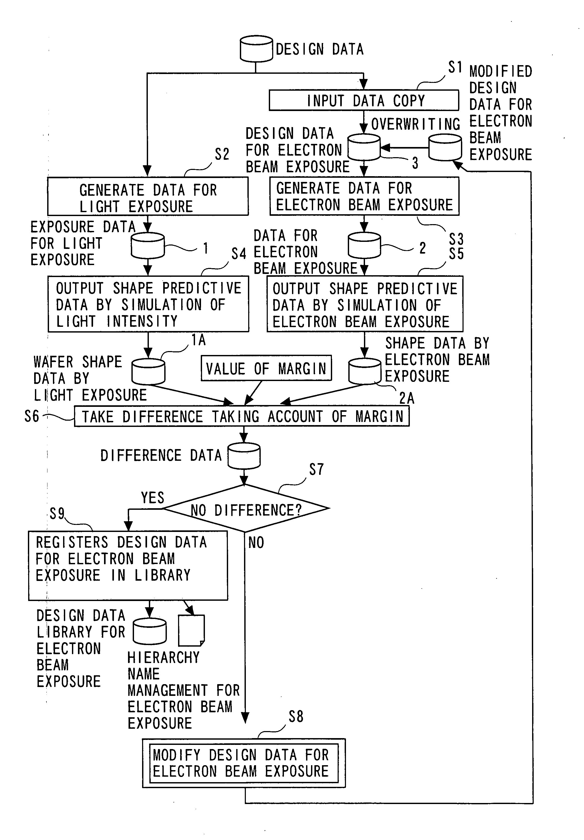
[0149]In the present embodiment, the embodiment has been described by exemplifying the light exposure technology and the electron beam exposure technology and can be also applied to combinations of other types of technologies.
[0150]>
[0151]A program for making a computer, other machines, devices (which will hereinafter be referred to as the computer etc) actualize any one of the functions given above, can be recorded on a recording medium readable by the computer etc. Then, the computer etc is made to read and execute the program on this recording medium, whereby the function thereof can be provided.
[0152]Herein, the recording medium readable by the computer etc connotes a recording medium capable of storing information such as data and programs electrically, magnetically, optically, mechanically or by chemical action, which can be read from the computer etc. Among these recording mediums, for example, a flexible disc, a magneto-optic disc, a CD-ROM, a CD-R / W, a DVD, a DAT, an 8 mm t...
PUM
| Property | Measurement | Unit |
|---|---|---|
| shape | aaaaa | aaaaa |
| electron beam exposure simulation | aaaaa | aaaaa |
| dimension | aaaaa | aaaaa |
Abstract
Description
Claims
Application Information