Manufacturing method of light-emitting device

a manufacturing method and light-emitting technology, applied in the direction of semiconductor/solid-state device details, electrical equipment, coatings, etc., can solve the problems of difficult method use, limited layer thickness distribution and variation, and difficult to improve etc., to achieve the effect of reducing the risk of deterioration, and improving the accuracy of positional alignment for selective deposition

Inactive Publication Date: 2008-10-30
SEMICON ENERGY LAB CO LTD
View PDF19 Cites 54 Cited by
  • Summary
  • Abstract
  • Description
  • Claims
  • Application Information

AI Technical Summary

Benefits of technology

[0018]According to the present invention, a positional alignment for selective deposition can be enhanced and the interval between pixels emitting different colors can be designed to be narrow, and accordingly still higher definition can be realized in a full-color display device.
[0050]In the deposition method of the present invention, a region evaporated by a heat source or the amount of a material to be evaporated is small, and thus attachment of the evaporated material to the inner wall of a deposition chamber can be suppressed. Accordingly, the frequency of cleaning the deposition chamber can be reduced.

Problems solved by technology

There are strict limitations to distribution and variations of thicknesses of layers including an organic compound used for organic EL elements.
Further, there is a possibility that characteristics of the layers including an organic compound may deteriorate due to impurities such as moisture when they are exposed to the air.
Therefore, because the thickness of a layer including an organic compound used for an organic EL element is small, it is difficult to use a method in which a photoresist having a desired pattern formed by light exposure and development is formed over such a layer including an organic compound, and then the layer including an organic compound is selectively etched using the formed photoresist as a mask.

Method used


Image

  • Manufacturing method of light-emitting device
  • Manufacturing method of light-emitting device
  • Manufacturing method of light-emitting device

Examples


embodiment modes

[0063]Embodiment Modes of the present invention will now be described.

embodiment mode 1

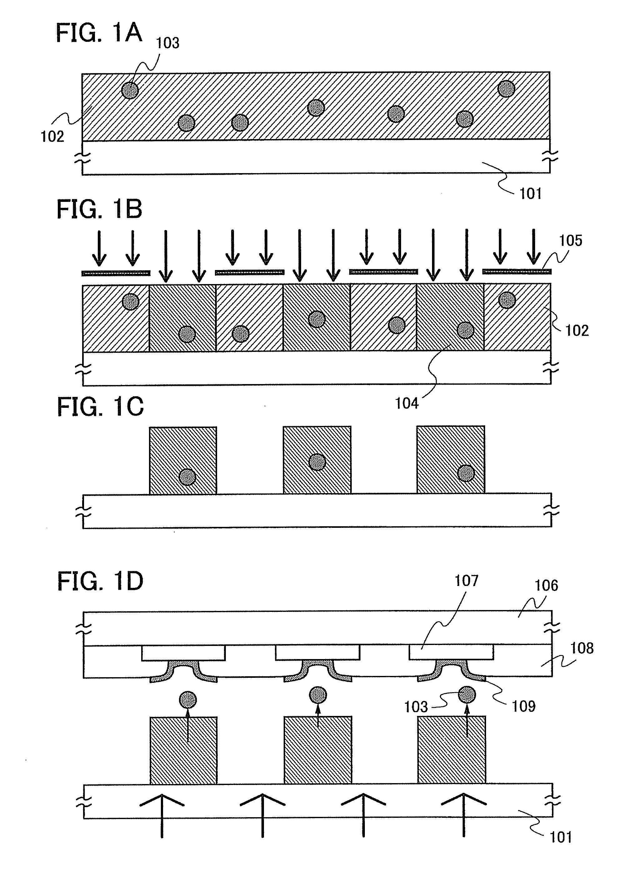
[0064]A manufacturing method of a light-emitting device is described with reference to FIG. 1A to FIG. 1D.

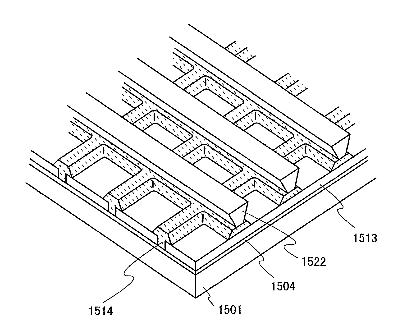
[0065]A first substrate 106 and a second substrate 101 are prepared first. The first substrate 106 is a substrate to be provided with a light-emitting element, and the second substrate 101 is a substrate used for forming a second layer including an organic compound over the first substrate 106 (the second substrate 101 is also referred to as a plate). As the second substrate 101, a substrate having a light-transmitting property can be used.

[0066]On the second substrate 101, an application liquid, i.e., a liquid in which an organic compound 103 (or a precursor of the organic compound 103) is dissolved or dispersed in a solvent is applied by a wet process, e.g., a spin coating method, a spray coating method, a dip coating method or the like. The organic compound 103 is preferably soluble or dispersible in the solvent. The thickness and uniformity of the second layer to be formed o...

embodiment mode 2

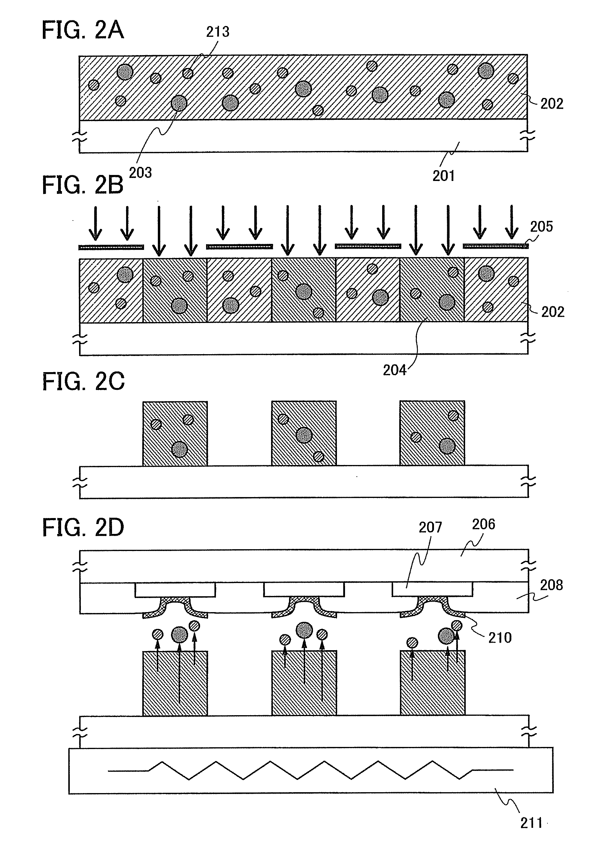
[0086]Plural types of organic compounds can be used, although Embodiment Mode 1 has described the example in which one type of organic compound is used. Embodiment Mode 2 will describe an example in which co-deposition is conducted using plural types of organic compounds.

[0087]A first substrate 206 and a second substrate 201 are prepared first. The first substrate 206 is a substrate to be provided with a light-emitting element, and the second substrate 201 is a substrate used for forming a second layer 210 including plural types of organic compounds over the first substrate 206. As the second substrate 201, a quartz substrate, a glass substrate, a ceramic substrate, a metal substrate or the like can be used.

[0088]On the second substrate 201, an application liquid, i.e., a liquid in which a first organic compound 203 (or a precursor of the organic compound 203) and a second organic compound 213 (or a precursor of the organic compound 203) is dissolved or dispersed in a solvent is app...


PUM

PropertyMeasurementUnit
widthaaaaaaaaaa
distanceaaaaaaaaaa
distanceaaaaaaaaaa

Abstract

For a full-color flat panel display, demands for high definition, high aperture ratio and high reliability have been increasing. Therefore, increasing in the number of pixels and narrowing a pixel pitch have been major issues. According to the present invention, a layer including an organic compound is selectively formed with a light-exposure apparatus used in a photolithography technique without a resist mask. A material layer including a photopolymerization initiator, a material polymerized with the photopolymerization initiator, and an organic compound are formed on a plate, and then are exposed to light and selectively cured. A film-formation substrate is disposed so as to face the plate. The film-formation substrate or the material layer is heated so that the organic compound included in a region exposed to light or a region not exposed to light is evaporated to be selectively deposited on the surface of the film-formation substrate.

Description

BACKGROUND OF THE INVENTION[0001]1. Field of the Invention[0002]The present invention relates to a light-emitting device using a light-emitting element which can provide fluorescence or phosphorescence when an electric field is applied to the element in which a film including an organic compound (hereinafter also referred to as a layer including an organic compound) is provided between a pair of electrodes, and a manufacturing method thereof.[0003]Note that the “light-emitting device” includes image display devices, light-emitting devices, and light sources (including illumination devices). In addition, a module in which a connector, for example, an FPC (Flexible Printed Circuit), TAB (Tape Automated Bonding) tape, or a TCP (Tape Carrier Package), is attached to a light-emitting device; a module in which a printed circuit board is provided ahead of a TAB tape or a TCP; and a module in which an integrated circuit (IC) is directly mounted on a light-emitting device by a COG (Chip On G...

Claims


Application Information

Patent Timeline
Patent Type & Authority Applications(United States)
IPC IPC(8): B05D5/12
CPCH01L51/0003H01L51/56H01L51/0013H01L51/0011H10K71/12H10K71/18H10K71/166H10K71/00H01L23/142H10K50/13H10K50/15H10K50/11
Inventor YOKOYAMA, KOHEIIKEDA, HISAOSATO, YOSUKEAOYAMA, TOMOYAIBE, TAKAHIROHIRAKATA, YOSHIHARU
Owner SEMICON ENERGY LAB CO LTD
Why Eureka
Try Eureka