Substrate processing apparatus and substrate processing method

a substrate and processing apparatus technology, applied in lighting and heating apparatus, furniture, instruments, etc., can solve the problems of increased running cost, difficult to obtain a high accuracy of line width, and difficulty in uniform coating of anti-reflective film

Inactive Publication Date: 2005-01-11
TOKYO ELECTRON LTD
View PDF4 Cites 56 Cited by
  • Summary
  • Abstract
  • Description
  • Claims
  • Application Information

AI Technical Summary

Benefits of technology

According to an eighth aspect of the present invention, there is provided a substrate processing method for processing a substrate coated with a chemical amplification type resist and subjected to a light exposure treatment before the developing processing, comprising the steps of transferring a substrate into a substrate table, heating the substrate disposed on said substrate table, and forming an electric field in a manner to prevent the protons generated in the resist formed on the substrate from being scattered while the substrate is being heated.

Problems solved by technology

However, the heating device of the construction described above gives rise to the following problem.
In the TARC treatment, however, it is difficult to coat uniformly the antireflective film.
Also, if the line width is rendered further narrower, it is difficult to obtain a high accuracy of the line width.
In addition, the running cost is increased because the coating step is required.
On the other hand, in the post-exposure bake of a chemical amplification type resist, the initial distribution of protons (H+) in the portions of the resist corresponding to the light-exposed regions is not uniform.
As a result, it is difficult for the chain reaction to take place uniformly so as to make it difficult to ensure a desired uniformity in the line width.
It should also be noted that, since the initial distribution of the acid of protons (H) is not uniform as described above, it is necessary to set the light exposure amount at a high level so as to prevent the portion where proton (H+) is deficient from being formed, leading to the waste of energy.
In addition, an inconvenience such as transpiration of the acid of proton (H+) is brought about as described above.
In the conventional post-exposure bake treatment, however, it is difficult to form an appropriate proton (H+) distribution conforming to the pattern.

Method used


Image

  • Substrate processing apparatus and substrate processing method
  • Substrate processing apparatus and substrate processing method
  • Substrate processing apparatus and substrate processing method

Examples


first embodiment

FIG. 3 is a cross sectional view showing the construction of the substrate processing apparatus according to the present invention. The substrate processing apparatus shown in the drawing is for applying a heat treatment to the substrate coated with a chemical amplification type resist and subjected to a light exposure treatment.

The substrate processing apparatus comprises a substrate table 1 on which is disposed a substrate coated with a chemical amplification type resist 2 and subjected to a light exposure treatment, e.g., a semiconductor wafer W. The substrate table 1 is made of, for example, a ceramic material. A heater 13, e.g., a resistance heat generator, for heating the wafer W disposed on the substrate table 1 from the back side of the wafer W is concentrically buried in the substrate table 1. Projections 17 are formed in that portion of the substrate table 1 which corresponds to the outer circumferential portion of the wafer W so as to permit a small clearance, e.g., a cle...

third embodiment

the present invention will now be described.

In the third embodiment of the present invention, a substrate table 1a made of a conductive material is arranged in place of the substrate table 1 shown in FIG. 3, and the negative side of the DC power supply 52 is connected directly to the substrate table 1a so as to allow the substrate table 1a to perform the function of the electrode, as shown in FIG. 8. In this case, the distance between the substrate table 1a acting as the electrode and the wafer W is set at, for example, 0.1 mm and voltage of scores of kV is applied between the substrate table 1a and the wafer W. Incidentally, it is necessary in this case to insulate the heater 13 and the substrate table 1a by suitable means so as to prevent the electrical interference with the heater 13.

fourth embodiment

the present invention will now be described with reference to FIGS. 9 and 10.

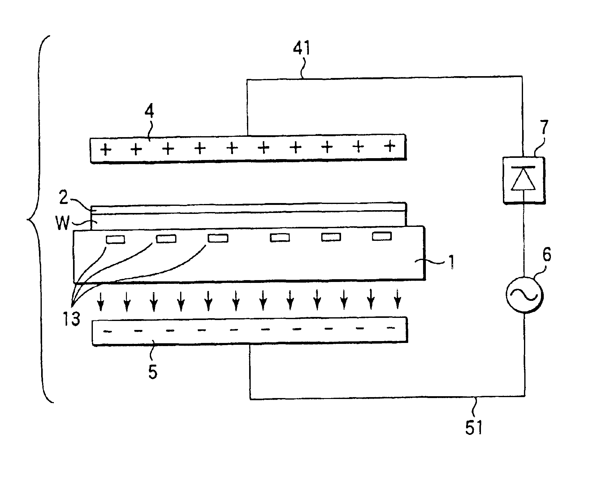
In the fourth embodiment of the present invention, an electrode is arranged on each of the front surface side and the back surface side of the wafer W. FIG. 9 is directed to the combination of the construction in the first embodiment of the present invention, in which the electrode 4 is arranged on the front surface side of the wafer W, and the construction in the second embodiment of the present invention, in which the electrode 5 is arranged on the back surface side of the wafer W. In this case, a repulsive force is exerted on the protons (H+) in the surface portion of the resist 2 from above and an attractive force is exerted on the protons (H+) from below so as to make it possible to suppress more effectively the scattering of the acid of protons (H+) from the surface portion of the resist 2.

In the example shown in FIG. 10, the electrodes 4 and 5 are arranged on the front surface side and the back surfa...


PUM

PropertyMeasurementUnit
temperatureaaaaaaaaaa
distanceaaaaaaaaaa
distanceaaaaaaaaaa

Abstract

A substrate processing apparatus for processing a substrate coated with a chemical amplification type resist and subjected to a light-exposure treatment comprises a substrate table on which is disposed a substrate, a heater for heating the substrate disposed on the substrate table, and an electric field forming mechanism for forming an electric field exerting force, which is directed toward the substrate, on the protons generated in the resist formed on the substrate disposed on the substrate table.

Description

BACKGROUND OF THE INVENTION1. Field of the InventionThe present invention relates to a substrate processing apparatus and a substrate processing method, in which a substrate is coated with a chemical amplification type resist, followed by exposing the resist to light and subsequently processing the substrate before the developing processing.2. Description of the Related ArtIn a photolithography step, which is one of the steps of the semiconductor device manufacturing process, a semiconductor wafer is coated with a thin resist film, followed by exposing the resist film to light in a prescribed pattern and subsequently developing the patterned resist film so as to form a mask pattern. These processes are carried out in general by using a system including a resist coating-developing device, and a light exposure device connected to the resist coating-developing device.On the other hand, a chemical amplification type resist material is being studied in recent years. In the chemical ampli...

Claims


Application Information

Patent Timeline
Patent Type & Authority Patents(United States)
IPC IPC(8): G03F7/38G03F7/038G03F7/039
CPCG03F7/38G03F7/0382G03F7/0392
Inventor NISHI, TAKANORISHIRAKAWA, EIICHI
Owner TOKYO ELECTRON LTD
Why Eureka
Try Eureka