Organic electroluminescent element and device

a technology of electroluminescent elements and organs, applied in the direction of discharge tubes/lamp details, luminescent compositions, discharge tubes/lamp details, etc., can solve the problems of radical deterioration of luminescent efficiency, and inability to achieve large improvement of luminescent efficiency

Active Publication Date: 2008-03-06
UDC IRELAND
View PDF2 Cites 91 Cited by
  • Summary
  • Abstract
  • Description
  • Claims
  • Application Information

AI Technical Summary

Benefits of technology

[0010]The present invention has been made in view of the above circumstances and provides an organic electroluminescent element comprising at least a positive hole transport layer, a light emitting layer and an electron transport layer between at least a pair of electrodes, wherein the light emitting layer contains therein at least two light emitting materials having different electron affinity (abbreviated to Ea values) or ionization potentials (abbreviated to Ip values) and emi

Problems solved by technology

However, large improvement in luminescent efficiency could not be expected by those means.
However, large improvement in luminescent efficiency could not be expected.
However, it has been revealed that the organic EL element using the phosphorescence

Method used


Image

  • Organic electroluminescent element and device
  • Organic electroluminescent element and device
  • Organic electroluminescent element and device

Examples


example 1

1. Measurements of Ea Values, Ip Values and Light Emission Spectra for Light Emitting Materials

(Measurements of Ea Values and Ip Values)

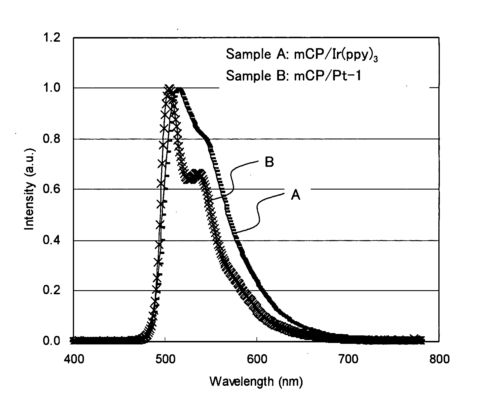
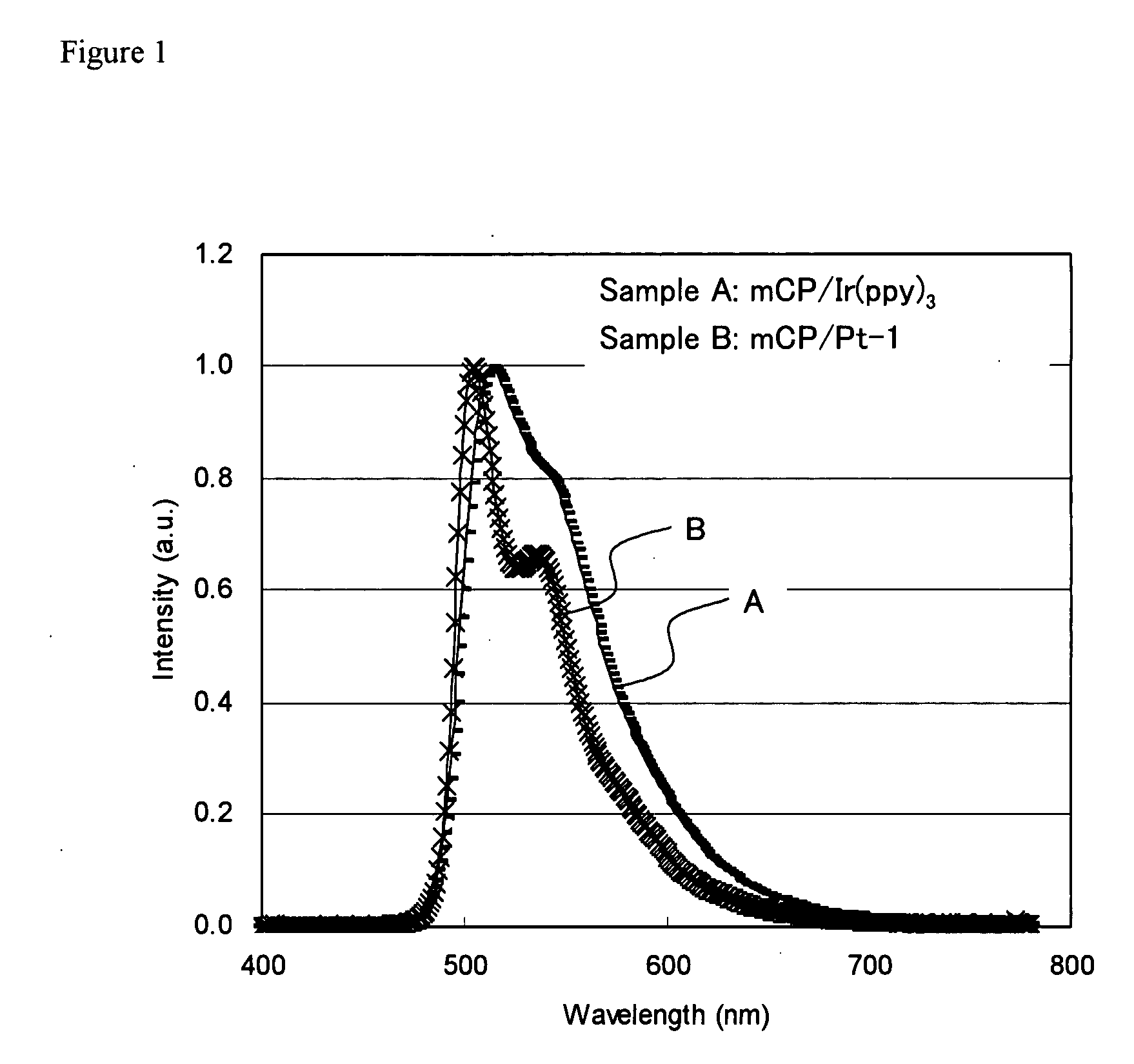
[0186]Ea values and Ip values of three light emitting materials, such as mCP, Ir(ppy)3 and platinum complex Pt-1, were measured as follows.

[0187]Films for measurement were prepared by a vapor deposition on a glass substrate at a film thickness of 100 nm. Ip value of the obtained samples was measured by Spectrophotometer AC-2 (manufactured by Riken Keiki Co., Ltd.) at a light intensity of 20 nW under an ambient atmospheric environment.

[0188]Further, films for measurement were prepared by a vapor deposition on a quartz substrate at a film thickness of 100 nm. A spectral absorption of samples obtained over wavelengths of 180 nm to 700 nm was measured by using a Hitachi Spectrophotometer Model U3310 (manufactured by Hitachi Ltd.). Then, an energy gap value (Eg(ev)) was calculated from the absorption end of the obtained absorption spectrum at the longest...

example 2

1. Preparation of Organic EL Element

[0224]1) Preparation of Comparative Organic EL Element No. B1

[0225]A glass substrate having a thickness of 0.5 mm and a rectangular of 2.5 cm was put in a washing vessel, and washed with ultrasonic in 2-propanol, followed by an UV-ozone treatment for 30 minutes. The following layers were diposited on the transparent anode by a vacuum evaporation method. The evaporation speed of the vacuum evaporation method in Examples of the present invention is usually 0.2 nm / second unless it is insisted. The evaporation speed was measured by using a quartz resonator. The film thicknesses described below were also measured by the quartz resonator.

[0226]Anode: ITO (Indium Tin Oxide) was desposited on a grass substrate to have a film thickness of 100 nm.

[0227]Positive hole injection layer: 2-TNATA was deposited on the anode (ITO) at a film thickness of 100 nm.

[0228]Positive hole transport layer: α-NPD was desposited on the positive hole injection layer at a film t...

example 3

[0246]Organic EL element Nos. 4-12 were prepared in the same manner as that in the organic EL element No. 3, except that a composition of the light emitting layers and the other layers was changed as described in Table 5. The samples obtained were evaluated in the same manner as that in Example 2.

[0247]As is apparent from Table 5, it is noted that the organic EL elements of the present invention provide extremely high external quantum efficiency at a high light emission, and thereby, it results to save a consumption of an electric power through driving at a high current density.

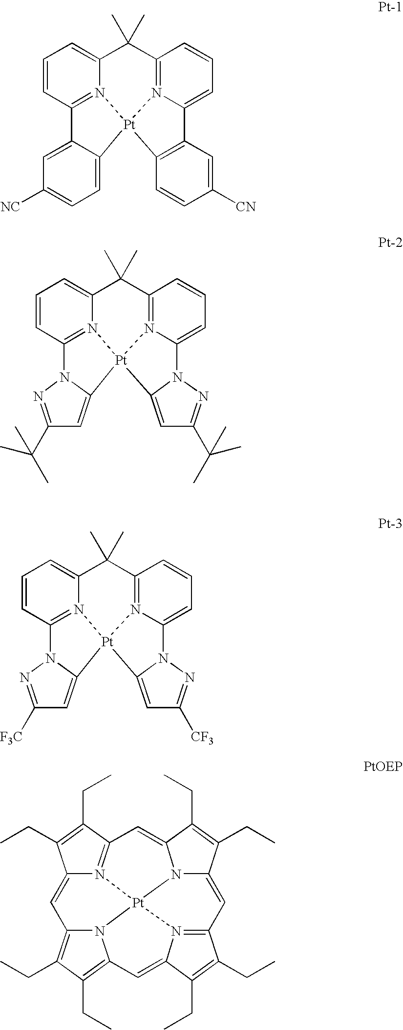
TABLE 5ExternalQuantumEfficiencyFirst Light Emitting LayerThird Light Emitting Layeratat(Adjacent to Hole TransportThicknessSecond LightThickness(Adjacent to ElectronThickness1,0001,000Sample No.Layer)(nm)Emitting Layer(nm)Transport Layer)(nm)cd / m2cd / m2Inventive Sample No. 4mCP / 15% by weight Pt-115——mCP / 8% by weight156.3%9.3%Ir(ppy)2(ppz)Inventive Sample No. 5mCP / 3% by weight PtOEP15——mCP / 6% by weight153.3%7....


PUM


Abstract

An organic electroluminescent (EL) element includes at least a positive hole transport layer, a light emitting layer and an electron transport layer between at least a pair of electrodes, wherein the light emitting layer contains therein at least two light emitting materials having different Ea values or Ip values and emitting phosphorescence having the same color as each other, and among the two light emitting materials, a light emitting material having a larger Ea value or Ip value is contained at a higher density in a region of the light emitting layer in the vicinity of the positive hole transport layer, while a light emitting material having a smaller Ea value or Ip value is contained at a higher density in a region of the light emitting layer in the vicinity of the electron transport layer.

Description

CROSS REFERENCE TO RELATED APPLICATION [0001]This application claims priority under 35 USC 119 from Japanese Patent Application Nos. 2006-242,080, 2006-242,081 and 2007-131,640, the disclosures of which are incorporated by reference herein.BACKGROUND OF THE PRESENT INVENTION[0002]1. Field of the Present Invention[0003]The present invention relates to an organic electroluminescent element and a display device using the same which can be effectively applied to a surface light source for full color display, backlight, illumination light sources and the like; or a light source array for printers, and the like.[0004]2. Description of the Related Art[0005]An organic electroluminescence element (hereinafter, referred to as an “organic EL element” in some cases) is composed of a light emitting layer or a plurality of organic layers containing a light emitting layer, and a pair of electrodes sandwiching the organic layers. The organic EL element is an element for obtaining luminescence by ut...

Claims


Application Information

Patent Timeline
IPC IPC(8): H01J1/63
CPCC09K11/06C09K2211/1029C09K2211/1044C09K2211/1092C09K2211/185H05B33/14H01L51/0072H01L51/0081H01L51/0085H01L51/0087H01L51/5016H01L51/0059H10K85/631H10K85/6572H10K85/346H10K85/324H10K85/342H10K50/11H10K2101/10
Inventor SATOU, TASUKU
Owner UDC IRELAND
Why Eureka
Try Eureka