Level shifting circuit, driving device, LED print head, and image forming apparatus

a level shifting circuit and driving device technology, applied in logic circuit coupling/interface arrangement, pulse automatic control, pulse technique, etc., can solve the problems of insufficient use of feature fabrication process used to fabricate logic circuits, insufficient space occupation, and insufficient space occupation

Inactive Publication Date: 2008-03-06
OKI DATA CORP
View PDF5 Cites 46 Cited by
  • Summary
  • Abstract
  • Description
  • Claims
  • Application Information

AI Technical Summary

Benefits of technology

[0018]Like the first level-shifting circuit, the second level-shifting circuit does not have to withstand the full voltage difference between the reference voltage and the second voltage. The pre-buffer circuits can accordingly be fabricated by a fine-featured process and the driving device can be small in size, hence relatively inexpensive.

Problems solved by technology

A problem when low-voltage logic and higher-voltage driving circuits are combined in the same IC chip is that the fine-featured fabrication process used to fabricate the logic circuits cannot be used to fabricate the high-voltage driving circuits; separate processes must be used, so the fabrication process for the entire chip becomes very lengthy, involving many different steps.
Another problem is that high-voltage MOS FETs must have a greater gate length than the MOS FETs in the logic circuits, so they take up an inordinate amount of space, and prevent the size and hence the cost of the chip from being reduced.

Method used


Image

  • Level shifting circuit, driving device, LED print head, and image forming apparatus
  • Level shifting circuit, driving device, LED print head, and image forming apparatus
  • Level shifting circuit, driving device, LED print head, and image forming apparatus

Examples


first embodiment

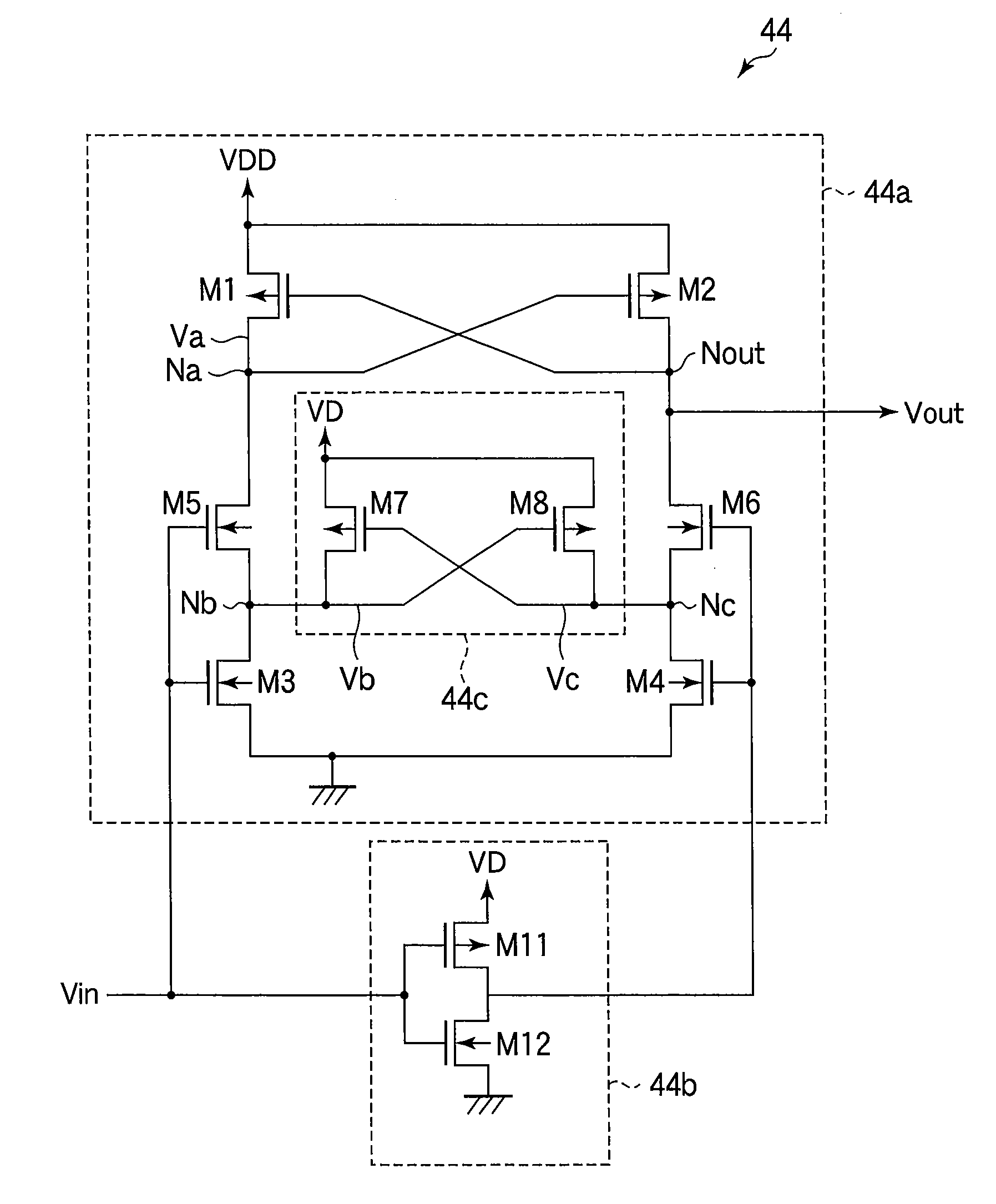
[0070]The first embodiment is a level shifting circuit that can be used in the level converter 44 in FIG. 4.

[0071]Referring to FIG. 5, the level shifting circuit 44a according to the first embodiment forms one part of the level converter 44, the other part being a level inverting circuit 44b. The level shifting circuit 44a includes a clamping circuit 44c connected to a first node Nb and a second node Nc. Reference characters M1, M2, M7, M8, and M11 indicate PMOS transistors; reference characters M3 to M6 and M12 indicate NMOS transistors.

[0072]PMOS transistor M1 has a source terminal connected to the second power supply voltage VDD (more precisely, to a power supply terminal that supplies the second supply voltage VDD), a drain terminal connected to the drain terminal of NMOS transistor M5 at a third node Na, and a gate terminal connected to the drain terminals of PMOS transistor M2 and NMOS transistor M6 at a fourth node Nout from which the shifted output signal Vout of the level s...

second embodiment

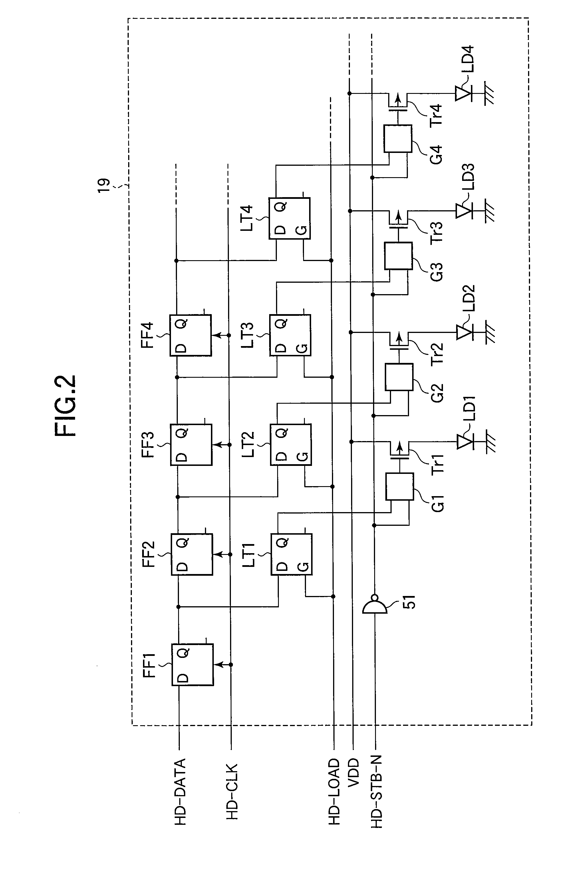
[0086]The second embodiment is a driver IC having pre-buffers with the circuit structure shown in FIG. 4, including the level converter 44 shown in FIG. 5.

[0087]Referring to FIG. 7A, pre-buffer G1 can be regarded as comprising an input buffer 101 that receives the input signal Vin and outputs a signal S0, a first level shifting circuit 102 that receives signal S0 and outputs a signal S1, and a second level shifting circuit 103 that receives signal S1 and outputs a signal S2. The levels of the respective output signals S0, S1, S2 are illustrated schematically in FIG. 7B: output signal S0 swings between ground level (0 V) and the first supply voltage VD; output signal S1 swings between ground level (0 V) and the second supply voltage VDD; output signal S2 swings between the control voltage Vcont and the second supply voltage VDD.

[0088]FIG. 8 relates the simplified block diagram in FIG. 7A to the circuitry shown in FIGS. 4 and 5. The level inverting circuit 44b in FIG. 5 is seen to cor...

third embodiment

[0112]FIG. 11 is a sectional view of an LED print head 1200 illustrating a third embodiment of the invention.

[0113]The LED print head 1200 includes a base member 1201 with an inverted U-shape. An LED unit 1202 is mounted on a base member 1201. The LED unit 1202 has, for example, twenty-six driver ICs including LED driving circuits as shown in the second embodiment (FIG. 9) mounted on a printed wiring board. FIG. 12 is a plan view showing an example of the LED unit 1202, where twenty-six LED array chips 1202a, each including 192 light-emitting diodes arranged in a line, are mounted in the longitudinal direction on the printed wiring board 1202e. The areas 1202b, 1202c indicated by the dotted lines on the printed wiring board 1202e are used for mounting and interconnecting the twenty-six driver IC chips and other electronic components (not shown). The twenty-six driver IC chips (not shown) are mounted facing the twenty-six LED array chips. The LED unit 1202 also includes a connector 1...


PUM


Abstract

A level shifting circuit converts an input signal that varies between ground and a first voltage to a shifted signal that varies between ground and a second voltage higher than the first voltage. The level shifting circuit has two branches, in each of which a p-channel transistor and two n-channel transistors are connected in series between the second voltage and ground. When the two n-channel transistors in each branch are turned off, a clamping circuit clamps the node between them to the first voltage level, so that neither n-channel transistor has to withstand the full difference between the second voltage and ground. The level shifting circuit can accordingly be fabricated with transistors of small size, reducing the cost of driving circuits, light-emitting-diode print heads, and image forming apparatus in which the level shifting circuit is used.

Description

BACKGROUND OF THE INVENTION[0001]1. Field of the Invention[0002]The present invention relates to a level shifting circuit, a driving device using the level shifting circuit, and a light-emitting diode (LED) print head and image forming apparatus incorporating the driving device.[0003]2. Description of the Related Art[0004]There are various types of conventional image forming apparatus, including image display apparatus and image recording apparatus such as printers, that employ semiconductor chips in which arrays of LEDs or other light-emitting elements are formed. These light-emitting element array chips are driven by integrated circuit (IC) chips in which driving circuits are formed, the light-emitting element array chips and driver ICs generally being mounted side by side. To meet the growing demand for high resolution in image forming apparatus, the density of the arrays and their driving circuits has increased markedly.[0005]Driver ICs in particular are now manufactured by semi...

Claims


Application Information

Patent Timeline
Patent Type & Authority Applications(United States)
IPC IPC(8): H03K19/0185H03L5/00
CPCH03K3/356104
Inventor NAGUMO, AKIRA
Owner OKI DATA CORP
Why Eureka
Try Eureka