Magnetoresistance effect device

a technology of magnetic field and effect, which is applied in the field of magnetic field, can solve the problems of less suitable mass production process, and achieve the effects of excellent properties, extremely high mr ratio, and excellent properties

Inactive Publication Date: 2008-03-06
ANELVA CORP +1
View PDF41 Cites 35 Cited by
  • Summary
  • Abstract
  • Description
  • Claims
  • Application Information

AI Technical Summary

Benefits of technology

[0014] An object of the present invention is to provide a magnetoresistance effect device having a high MR ratio, improving the mass producibility, and improving the practicality and a method of production of the same.
[0017] According to above magnetoresistance effect device, since the barrier layer has a single crystal or highly oriented fiber-texture structure, the flow of current between the ferromagnetic layers can be made straight and the MR ratio can be made an extremely high value.
[0022] According to the present invention, since the tunnel barrier layer forming the intermediate layer of the TMR device or other magnetoresistance effect device is an MgO layer having a single crystal or highly oriented fiber-texture structure, the MR ratio can be made extremely high. When using this as a memory device of an MRAM, a gigabit class ultra-high integrated MRAM can be realized. Further, by forming the a single crystal or highly oriented fiber-texture MgO layer by the sputtering method, it is possible to fabricate a magnetoresistance effect device suitable for mass production and having high practical applicability.

Problems solved by technology

Further, epitaxial growth of an Fe film by an expensive MBE device, formation of an MgO film by ultrahigh vacuum electron beam evaporation and other sophisticated film deposition technology are required.
There is the problem that the longer the film deposition time, the less suitable the process for mass production.

Method used


Image

  • Magnetoresistance effect device
  • Magnetoresistance effect device
  • Magnetoresistance effect device

Examples


Embodiment Construction

[0030] Below, a preferred embodiment of the present invention will be explained with reference to the attached drawings.

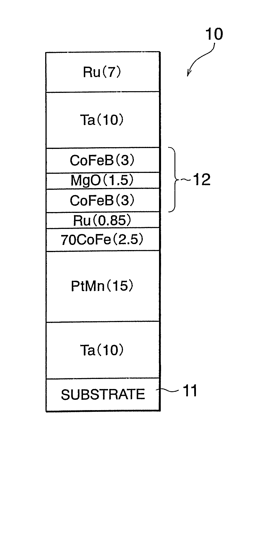
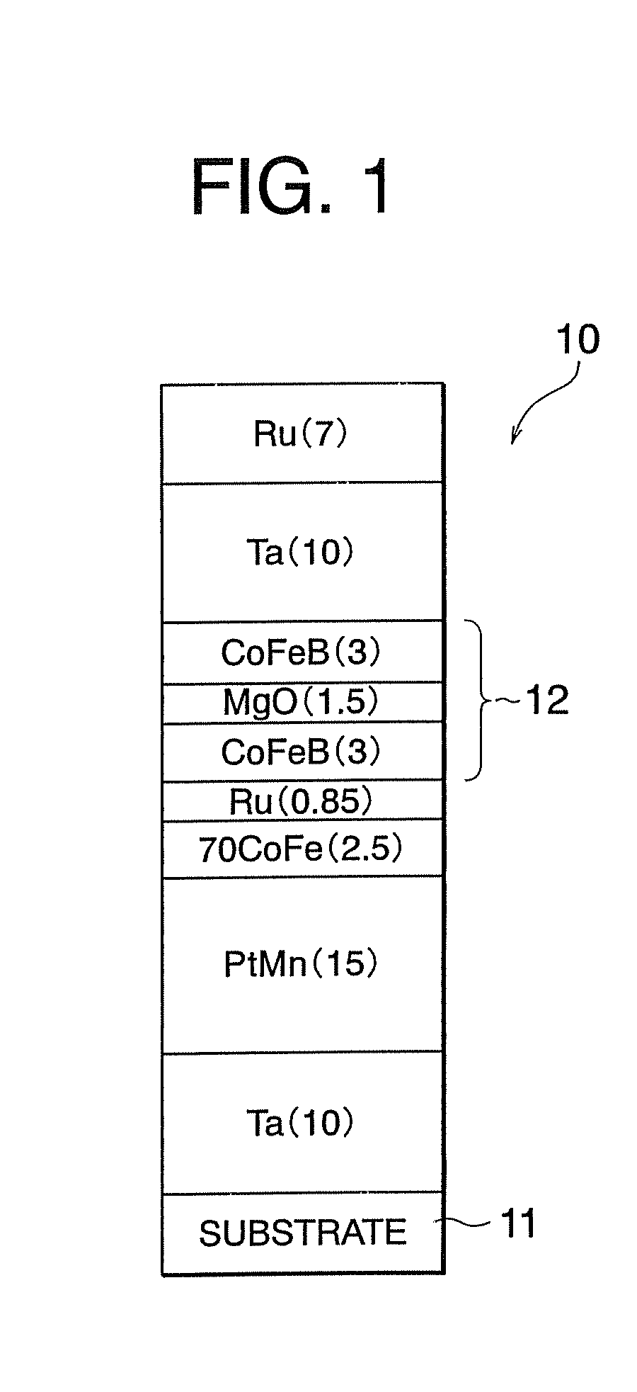
[0031]FIG. 1 shows an example of the multilayer structure of a magnetoresistance effect device according to the present invention, in particular shows the multilayer structure of a TMR device. According to this TMR device 10, a substrate 11 is formed with a multilayer film comprised of for example nine layers forming the TMR device 10. In this nine-layer multilayer film, magnetic films etc. are stacked from the bottommost first layer to the topmost ninth layer with “Ta”, “PtMn”, “70CoFe”, “Ru”, “CoFeB”, “MgO”, “CoFeB”, “Ta”, and “Ru” in that order. The first layer (Ta: tantalum) is an undercoat layer, while the second layer (PtMn) is an anti-ferromagnetic layer. The layers from the third layer to the fifth layer (70 CoFe, Ru, CoFeB) form fixed magnetization layers. The substantive fixed magnetization layer is the fifth layer ferromagnetic layer comprised of “CoFeB...


PUM

PropertyMeasurementUnit
temperatureaaaaaaaaaa
pressureaaaaaaaaaa
crystal structureaaaaaaaaaa

Abstract

A magnetoresistance effect device including a multilayer structure having a pair of ferromagnetic layers and a barrier layer positioned between them, wherein at least one ferromagnetic layer has at least the part contacting the barrier layer made amorphous and the barrier layer is an MgO layer having a highly oriented texture structure.

Description

CROSS-REFERENCE TO RELATED APPLICATIONS [0001] This application is a divisional of U.S. application Ser. No. 11 / 219,866 filed on Sep. 7, 2005, which claims priority to Japanese Application No. 2004-259280 filed on Sep. 7, 2004, the entire contents of which are incorporated herein by reference.BACKGROUND OF THE INVENTION [0002] 1. Field of the Invention [0003] The present invention relates to a magnetoresistance effect device and a method of production of the same, more particularly relates to a magnetoresistance effect device fabricated utilizing a simple sputtering film-formation method and having an extremely high magnetoresistance ratio and a method of production of the same. [0004] 2. Description of the Related Art [0005] In recent years, as nonvolatile memories, magnetic memory devices called “magnetoresistive random access memories (MRAMs)” have come into attention and have started entering the commercial stage. MRAMs are simple in structure, so ultra-high density integration ...

Claims


Application Information

Patent Timeline
Patent Type & Authority Applications(United States)
IPC IPC(8): G11B5/33
CPCB82Y25/00B82Y40/00C23C14/081C23C14/34G11C11/16H01L43/12H01F10/3254H01F41/18H01F41/307H01L43/08H01F10/3204G11C11/161H10N50/10H10N50/01G11C11/15
Inventor DJAYAPRAWIRA, DAVID D.TSUNEKAWA, KOJINAGAI, MOTONOBUMAEHARA, HIROKIYAMAGATA, SHINJIWATANABE, NAOKIYUASA, SHINJI
Owner ANELVA CORP
Why Eureka
Try Eureka