Complementary metal-oxide-semiconductor device and fabricating method thereof

a technology of metal-oxidesemiconductor and semiconductor device, which is applied in the direction of semiconductor device, electrical apparatus, transistor, etc., can solve the problems of serious affecting device reliability and performance, and achieve the effect of effective promotion of reliability and device performan

Active Publication Date: 2008-03-13
UNITED MICROELECTRONICS CORP
View PDF4 Cites 122 Cited by
  • Summary
  • Abstract
  • Description
  • Claims
  • Application Information

AI Technical Summary

Benefits of technology

[0008]Accordingly, the object of the present invention is to provide a method of fabricating a complementary metal-oxide-semiconductor device in which the possibility of generation of poly bump, as described in the prior art and other problems derived there-from, may be reduced, and thereby reliability and device performance may be effectively promoted.
[0009]Another object of the present invention is also to provide a method of fabricating a complementary metal-oxide-semiconductor device to reduce the possibility of generation of poly bump, as described in the prior art and other problems derived there-from, and thereby promote reliability and performance of devices.
[0010]Still another object of the present invention is to provide a complementary metal-oxide-semiconductor device with improved reliability and performance of devices.
[0011]Yet another object of the present invention is to provide a complementary metal-oxide-semiconductor device with improved reliability and performance of devices.
[0032]Since the passivation layer in the present invention is a carbon-containing oxynitride layer with a low etching rate, the passivation layer can be avoided from being improperly removed during the device manufacturing process. Therefore, the generation of the poly bump and the various problems derived therefrom can be avoided. In addition, the thermal process of the present invention can densify the density of the passivation layer to decrease the etching rate of the passication layer. Hence, the thermal process is benefit to the later performed processes.

Problems solved by technology

Therefore, when a SiGe process is performed to form the SiGe layer filling in the trench, the SiGe layer is also formed on the exposed substrate surface and the top of the P-type gate structure, i.e., a so-called “poly bump”, which seriously affects reliability and performance of devices.

Method used


Image

  • Complementary metal-oxide-semiconductor device and fabricating method thereof
  • Complementary metal-oxide-semiconductor device and fabricating method thereof
  • Complementary metal-oxide-semiconductor device and fabricating method thereof

Examples


Embodiment Construction

[0037]Reference will now be made in detail to the present preferred embodiments of the invention, examples of which are illustrated in the accompanying drawings. Wherever possible, the same reference numbers are used in the drawings and the description to refer to the same or like parts.

[0038]FIGS. 1A to 1H are schematic sectional views illustrating a method of fabricating a complementary metal-oxide-semiconductor device according to one embodiment of the present invention.

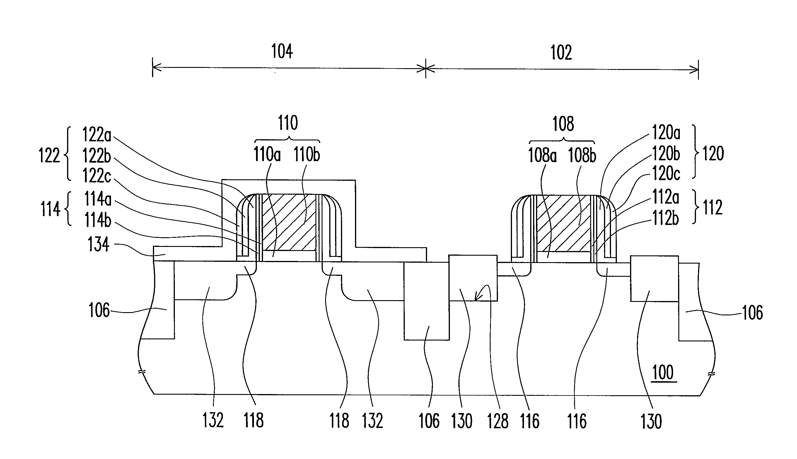
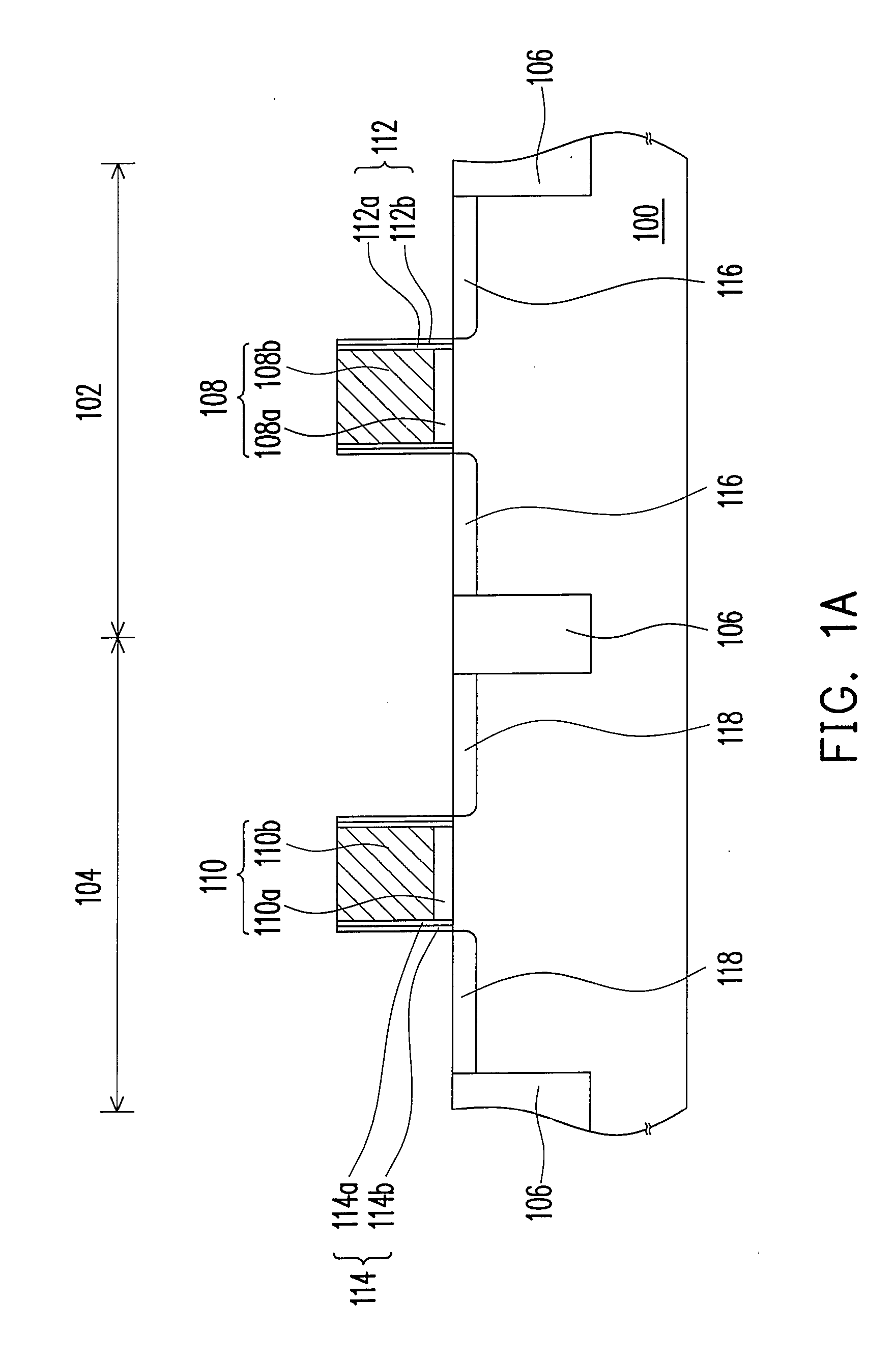
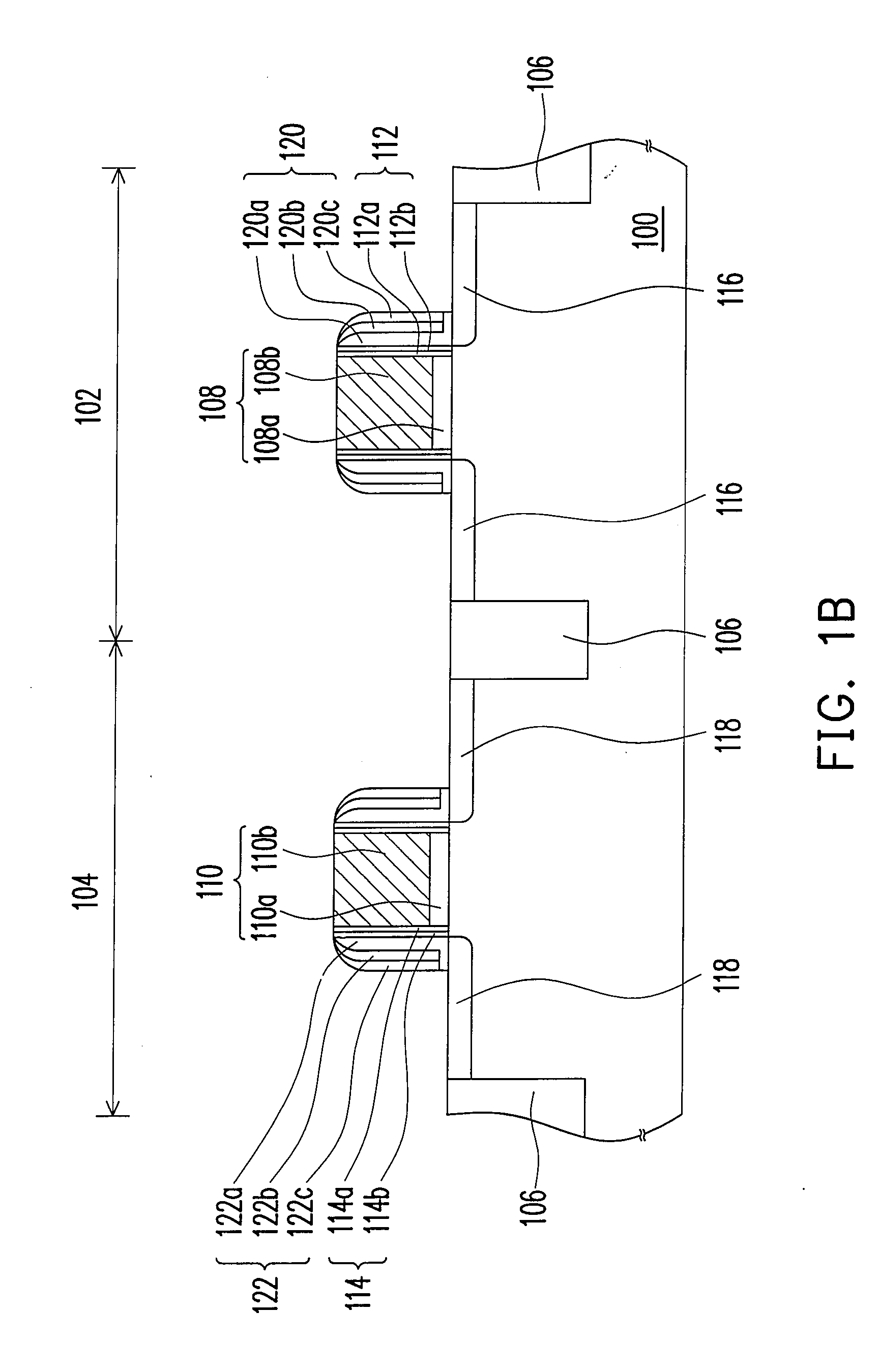
[0039]First, referring to FIG. 1A, a substrate 100 having a first active region 102 and a second active region 104 is provided, wherein the first active region 102 and the second active region 104 are separated by an isolation structure 106. The isolation structure 106 is, for example, a shallow trench isolation (STI) structure or any other suitable isolation structure. Next, a first gate structure 108 and a second gate structure 110 are formed on the first active region 102 and the second active region 104, respe...


PUM


Abstract

A complementary metal-oxide-semiconductor (CMOS) device includes a substrate with a first active region and a second active region; a first gate structure and a second gate structure, respectively disposed on the first active region and the second active region; a first spacer structure and a second spacer structure respectively disposed on sidewalls of the first gate structure and the second gate structure; a first LDD and a second LDD respectively disposed in the substrate at both sides of the first gate structure and the second gate structure; an epitaxial material layer, disposed in the first active region and located on a side of the first LDD; and a passivation layer, disposed on the first gate structure, the first spacer structure, and the first LDD and covering the second active region, wherein the passivation layer comprises a carbon-containing oxynitride layer.

Description

BACKGROUND OF THE INVENTION[0001]1. Field of the Invention[0002]The present invention relates to a semiconductor device and a forming method thereof, in particular, to a complementary metal-oxide-semiconductor device and a fabrication method thereof.[0003]2. Description of Related Art[0004]At present, a method of fabricating a source / drain (S / D) region of a complementary metal-oxide-semiconductor (MOS) transistor using a SiGe technique has been proposed to increase mobility of electrons and holes for improving the performance of devices.[0005]Generally, the method applying the SiGe technique to manufacturing a complementary metal-oxide semiconductor (CMOS) device comprises steps of forming a P-type gate structure and an N-type gate structure on the substrate and then forming a spacer and a lightly-doped drain (LDD) sequentially. Thereafter, a high-temperature oxide (HTO) layer is formed on the entire substrate. After that, a portion of HTO layer on the PMOS transistor region is remo...

Claims


Application Information

Patent Timeline
Patent Type & Authority Applications(United States)
IPC IPC(8): H01L29/76
CPCH01L21/823807H01L21/823814H01L21/823864H01L29/6656H01L29/7834H01L29/66636H01L29/7833H01L29/7843H01L29/6659
Inventor LIU, CHE-HUNGCHENG, PO-LUNLIN, CHUN-ANTANG, LI-YUENSHIH, HUNG-LINFAN, MING-CHIMENG, HSIEN-LIANGCHIANG, JIH-SHUN
Owner UNITED MICROELECTRONICS CORP
Why Eureka
Try Eureka