Plasma Display Panel And Production Method Therefor

a technology of display panel and plasma, which is applied in the manufacture of electric discharge tube/lamp, discharge tube luminescnet screen, electrode system, etc., can solve the problems of high technical potential of surface discharge ac type pdp device, long life, weak discharge, etc., and achieve high luminous efficiency, high image quality, and reduce the effect of panel luminous efficiency

Inactive Publication Date: 2008-03-13
PANASONIC CORP
View PDF7 Cites 23 Cited by
  • Summary
  • Abstract
  • Description
  • Claims
  • Application Information

AI Technical Summary

Benefits of technology

[0039] The inventors of the present invention found that a strong discharge is apt to be generated when the rising ramp waveform, among the ramp waveforms, is applied during the reset period, when PDPs with conventional structures are driven. More specifically, in the reset period, all cells are reset by first applying a rising ramp waveform voltage with a positive slant to the scan electrodes, and then applying a falling ramp waveform voltage. In this reset period, a reset discharge would become unstable and a strong discharge, namely an undesired discharge, would be generated when the rising ramp waveform voltage is applied when the data electrodes or the phosphor layers side having a small value of the secondary electron emission coefficient r becomes a cathode.
[0040] The above-described phenomenon taken into consideration, in the PDP of the present invention, the high γ members are formed to be exposed to the discharge spaces. With this arrangement, the firing voltage, when the ramp waveform is applied and when the phosphor layers side becomes a cathode during the reset period when the PDP is driven, is lowered, which restricts ...

Problems solved by technology

Among such PDP devices, surface discharge AC type PDP devices have high technical potential and are long in life.
This causes the weak discharge unstable, and makes a strong discharge apt to be generated.
This causes a problem that an erroneous light emission (hereinafter referred to as reset luminous point) occurs during the reset period, irrelevant to displaying of image.
However, if the rate of partial pressure of Xe to the total pressure of the discharge gas is increased, the luminous efficiency is improved, but the firing voltage increases, and when the ramp waveform is applied during the rese...

Method used


Image

  • Plasma Display Panel And Production Method Therefor
  • Plasma Display Panel And Production Method Therefor
  • Plasma Display Panel And Production Method Therefor

Examples


embodiment 1

1. Entire Structure of PDP 1

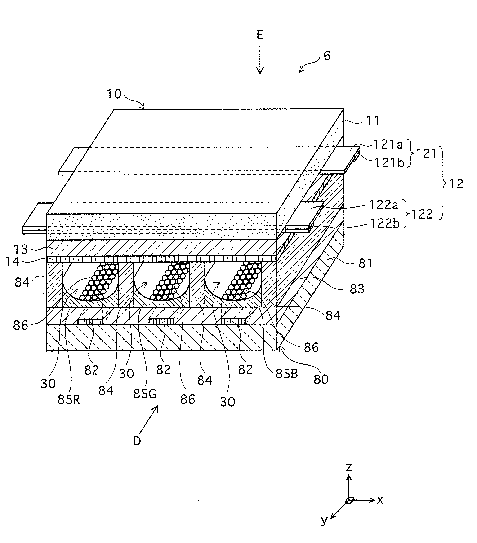
[0149] The entire structure of a PDP 1 of the present invention will be described with reference to FIG. 1. FIG. 1 is a main part perspective view showing the main part of the PDP 1.

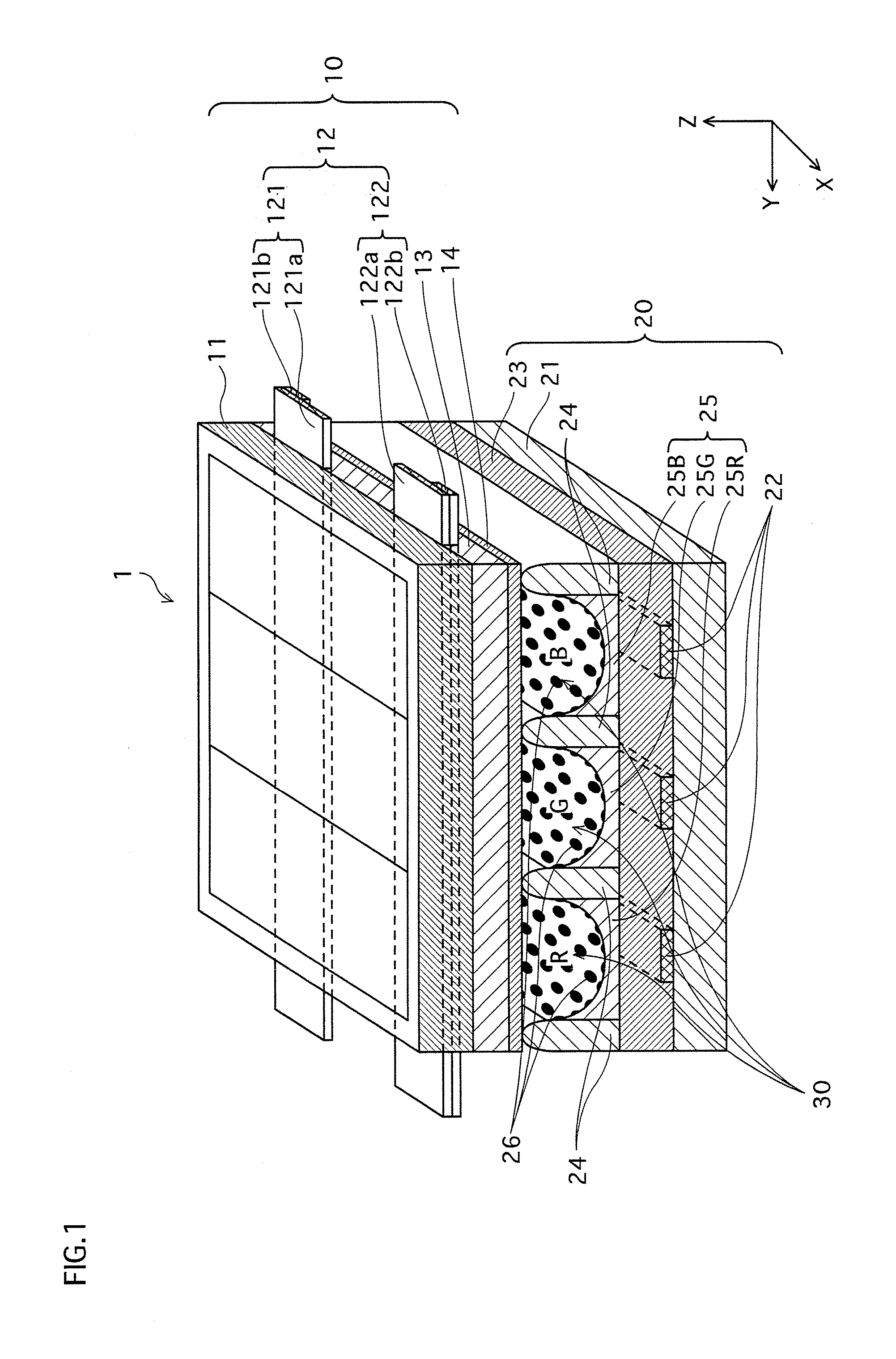
[0150] As shown in FIG. 1, the PDP 1 is composed of two major parts: a front panel 10 and a back panel 20. The front panel 10 is constructed such that a plurality of display electrode pairs 12 are disposed in parallel with each other on a main surface (in FIG. 1, the lower main surface facing downward in the Z axis direction) of a front substrate 11. And a dielectric layer 13 and a dielectric protective layer 14 are formed to cover the display electrode pairs 12, in the stated order. Each pair of the display electrode pairs 12 is made of a scan electrode (hereinafter referred to as Scn electrode) 121 and a sustain electrode (hereinafter referred to as Sus electrode) 122. The Scn electrode 121 is composed of a transparent electrode element 121a and a bus line 121b that are lam...

embodiment 2

[0185] The structure of a PDP 2 of Embodiment 2 will be described with reference to FIGS. 4A, 4B and 5. The front panel 10 and a back panel 40 excluding phosphor-coating films 46 are structured in the same manner as in Embodiment 1, and description thereof is omitted.

[0186] As shown in FIG. 4A, the phosphor-coating films 46 in the PDP 2 are formed on part of the surface of phosphor layers 45 as in Embodiment 1 in this sense, but are formed differently from the phosphor-coating films 26 in Embodiment 1 in that the phosphor-coating films 46 are formed in areas WDAT that are located directly above the Dat electrodes 42. Also, as shown in FIG. 4B that is a cross-sectional view taken along line A-A shown in FIG. 4A, the phosphor-coating films 46 are formed in areas WSCN that are located directly below the Scn electrodes 121 constituting the display electrode pairs 12 formed in the front panel 10.

[0187]FIG. 5 shows only the electrodes 121, 122, and 42, the barrier ribs 44, and the phosp...

embodiment 3

[0193] A PDP 3 of Embodiment 3 will be described with reference to FIG. 6. The front panel 10 and a back panel 50 excluding the high γ members are structured in the same manner as in Embodiments 1 and 2, and description thereof is omitted.

1. Structure of PDP 3

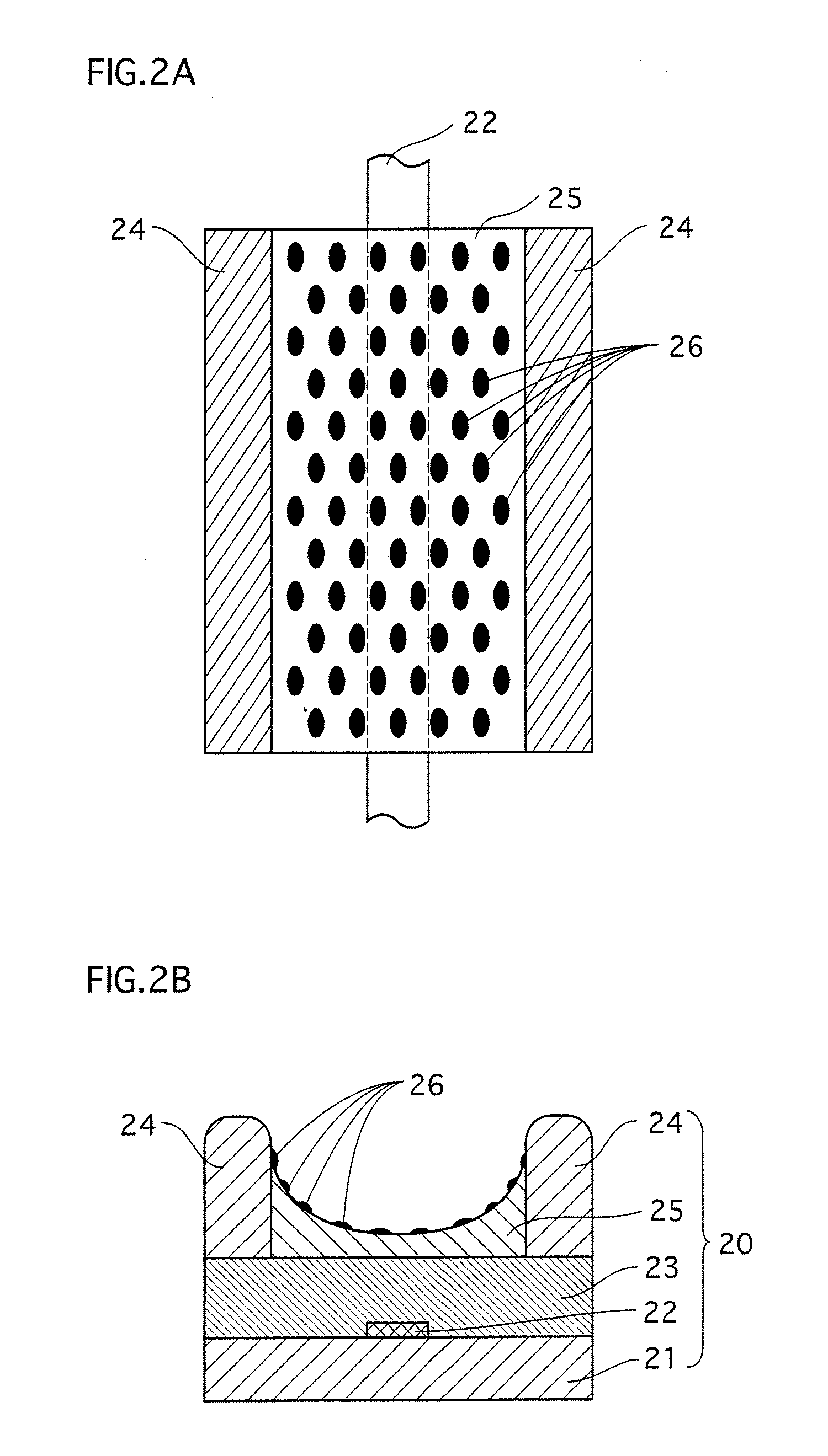
[0194] As shown in FIG. 6, in the PDP 3 of the present embodiment, particles 56 are attached to the surface of phosphor layers 55. The particles 56 are made of a material that has a higher value of the secondary electron emission coefficient γ than each phosphor material of the phosphor layers 55. For example, the particles 56 are made of the same material as the phosphor-coating films 26 disclosed in Embodiment 1. In the PDP 3 of the present embodiment, the portions where the particles 56 are formed on the surface of the phosphor layers 55 are the high γ members. As one example, the high γ members can be formed using a metal oxide such as MgO or SrO as the material. In this case, particles of the metal oxide that are in the ...


PUM


Abstract

A PDP capable of lowering a discharge initiating voltage with a weak discharge always stabilized during an initialization period even if a Xe partial pressure ratio to a total pressure in discharge gas is increased, improving an image quality with the occurrence of an initializing bright point prevented, preventing the lowering of a light emission efficiency and brightness, and improving brightness; and a production method for simply producing the PDP. The PDP comprises a front panel and a rear panel disposed facing each other with a discharge space provided between them. A fluorescent layer is formed in the area on the discharge space side of the rear panel, and a fluorescent film as a high γ portion is formed in part of the area of its surface. The fluorescent film is formed of a material higher in secondary electron emission coefficient γ than a fluorescent material constituting the fluorescent layer. Part of the surface of the fluorescent layer is covered with the fluorescent film, with the other part facing the discharge space.

Description

TECHNICAL FIELD [0001] The present invention relates to a plasma display panel and a manufacturing method thereof. BACKGROUND ART [0002] Plasma display panel devices (hereinafter referred to as PDP devices), which have been developed into products, are flat surface display devices that use radiations from gas discharges. The PDP devices includes a DC (direct current) type and an AC (alternate current) type. Among such PDP devices, surface discharge AC type PDP devices have high technical potential and are long in life. Here, the structure of PDPs (hereinafter referred to as PDPs) that are panel units of the PDP devices will be described with reference to FIG. 26A. FIG. 26A is a development perspective view (partially sectional view) showing the structure of a conventionally typical surface discharge AC type PDP. [0003] As shown in FIG. 26A, the PDP has a structure in which a front panel 710 and a back panel 720 are arranged to face each other. The front panel 710 includes a front su...

Claims


Application Information

Patent Timeline
IPC IPC(8): H01J17/49H01J9/02H05B33/10
CPCH01J1/74H01J11/42H01J11/12H01J9/20H01J11/32H01J2211/323
Inventor MIURA, MASANORIMORITA, YUKIHIROHASHIMOTO, SHINICHIROYOSHINO, KYOHEIMATSUSHITA, JUNKOGOTO, MASASHI
Owner PANASONIC CORP
Why Eureka
Try Eureka