Printed wiring board and electronic equipment

a wiring board and electronic equipment technology, applied in the direction of insulated conductors, cables, high-frequency circuit adaptations, etc., can solve the problems of spurious noise, transmission of spurious noise, and reception of spurious noise outside the desired frequency band, so as to reduce the influence of noise signals, suppress radiation noise, and maintain the quality of signals transmitted

Active Publication Date: 2008-03-13
CANON KK
View PDF4 Cites 11 Cited by
  • Summary
  • Abstract
  • Description
  • Claims
  • Application Information

AI Technical Summary

Benefits of technology

[0019]It is an object of the present invention to provide a printed wiring board and electronic equipment capable of reducing an influence of a noise signal occurring between a baseband portion and a high-frequency portion and also capable of suppressing a radiation noise, to thereby maintain the quality of signals transmitted through an interface.

Problems solved by technology

For this reason, such noise component leads to a malfunction of each IC.
Also, those high-frequency signals are radiated as a radiation noise into space by a conductor such as a ground, which also results in a factor that causes a malfunction.
In particular, when an odd-order distortion is generated in the vicinity of the transmission frequency, a spurious noise is transmitted.
Further, when the noise component is mixed in the low noise amplifier 151, a spurious noise which is outside of the desired frequency band is received.
Also, when the noise component large in amplitude is input to the low noise amplifier 151, the low noise amplifier is saturated, leading to deterioration in reception sensitivity.
However, according to the above-mentioned interference prevention method, the grounds of the blocks are disconnected from each other, and a return path cannot be formed on the printed wiring board for a signal transmitted through the interface.
However, the transmission line 136 connecting the blocks to each other does not have a suitable ground plane corresponding thereto, and a return path cannot be formed via a minimal route.
For this reason, signals that should be transmitted through the transmission line 136 may be extremely deteriorated in quality, or the signals may not be transmitted in the worst case.
The above-mentioned two blocks are connected to the power source of the electronic device to form a long path, which does not serve as an effective return path, either.
However, this technology removes higher harmonic waves of the clock falling into a receiving frequency band, and is not capable of dealing with an interference secondarily occurring in the radio portion.
Also, it is impossible to prevent a spurious noise secondarily generated in the transmitting portion.

Method used


Image

  • Printed wiring board and electronic equipment
  • Printed wiring board and electronic equipment
  • Printed wiring board and electronic equipment

Examples


first embodiment

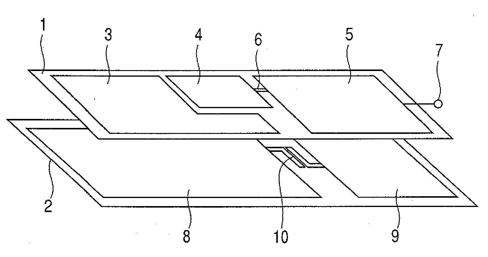
[0036]FIG. 1 is a schematic diagram for describing a structure of a printed wiring board, according to the present invention, of a digital camera having a built-in radio portion. A signal plane 1 has two blocks including a baseband block and a high-frequency block formed thereon. The baseband block includes a baseband signal processing portion 3 and a modulation / demodulation processing portion 4 which are electrically connected to each other. The high-frequency block includes a power amplifier 5. The modulation / demodulation processing portion 4 and the power amplifier 5 are connected to each other through a transmission line 6 which is an interface.

[0037]The baseband signal processing portion 3 has functions of executing digital signal processing on image information obtained with a CCD camera or the like, storing the image information, and outputting the image information. The baseband signal processing portion 3 generally performs operation and processing in synchronization with a...

second embodiment

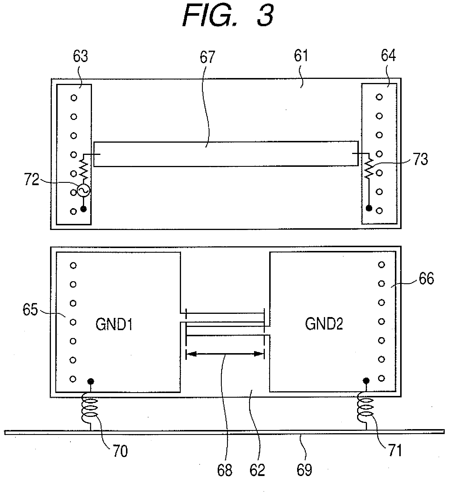
[0051]FIG. 7 illustrates a second Embodiment of the present invention. This embodiment illustrates a device for receiving an image taken by a digital camera or a digital video and transmitted by radio, and displaying or printing the image.

[0052]A printed wiring board according to this embodiment is provided with a signal plane 11 and a ground plane 12 for forming a circuit on both sides thereof. The signal plane 11 includes circuit function blocks and the ground plane 12 includes grounds corresponding to the blocks of the signal plane 11. A radio transmission signal input from a receiving antenna terminal 18 is amplified by a low-noise amplifier 16, and subjected to frequency conversion to have an intermediate frequency at the frequency converting portion 15. At this time, the frequency converting portion 15 is supplied with local signals by a local oscillation circuit 17 for frequency conversion, and arbitrarily selects frequencies of the local signal, to thereby select radio frequ...


PUM


Abstract

A printed wiring board, comprising a signal plane having a baseband block for processing a baseband signal and a high-frequency block for processing a high-frequency signal which is obtained by converting the baseband signal, and a ground plane opposing to the signal plane. The baseband block and the high-frequency block are connected through a transmission line for transmitting a signal of a specific frequency region. The ground plane is provided with a first ground portion and a second ground portion, the first ground portion being provided at an area opposing to the baseband block, the second ground portion being provided at an area opposing to the high-frequency block. The first ground portion and the second ground portion are coupled to each other through a coupling portion provided therebetween which has a low impedance with respect to the signal of the specific frequency region.

Description

BACKGROUND OF THE INVENTION[0001]1. Field of the Invention[0002]The present invention relates to a printed wiring board and electronic equipment capable of solving a problem of interference which takes place within the electronic equipment, in which electromagnetic waves generated by the electronic equipment affect the performance of the electronic equipment itself.[0003]2. Description of the Related Art[0004]In recent years, digital peripheral devices such as a digital camera or a printer are widespread, and personal computers or peripheral devices are connected to each other. Under such circumstances, a device, such as a digital camera and a printer, which has a built-in radio portion and enables connection to the peripheral device through a wireless interface is on the rise.[0005]FIG. 10 is a schematic diagram for explaining a structure of a digital camera having a radio portion incorporated therein. A printed wiring board 140 used for a digital camera is generally formed of two ...

Claims


Application Information

Patent Timeline
Patent Type & Authority Applications(United States)
IPC IPC(8): H04B1/00H04B1/10H04B1/40H05K1/02
CPCH05K1/0216H05K1/023H05K1/0237H05K2201/09972H05K2201/09236H05K2201/093H05K2201/09663H05K1/0239
Inventor TAKAHASHI, YASUHIRO
Owner CANON KK
Why Eureka
Try Eureka