Method for fabricating non-volatile memory

a non-volatile memory and semiconductor technology, applied in the direction of semiconductor devices, basic electric elements, electrical equipment, etc., can solve the problems of affecting the size the removal of the silicon nitride layer and the top oxide layer in the peripheral circuit area, and the device may become defective, so as to prevent the expansion of the buried diffusion region and improve the control of the device characteristics of the memory. , the effect of short channels

Inactive Publication Date: 2008-03-13
MACRONIX INT CO LTD
View PDF9 Cites 12 Cited by
  • Summary
  • Abstract
  • Description
  • Claims
  • Application Information

AI Technical Summary

Benefits of technology

[0008]In view of the foregoing, the present invention provides a method for fabricating a non-volatile memory in which the expansion of the buried diffusion region is prevented. Ultimately, the short channel effect is mitigated and the device characteristics of the memory can be better controlled.
[0009]The present invention also provides a method for fabricating a non-volatile memory, wherein the gate insulating layer of the low voltage devices in the peripheral circuit area is obviated of defects. Consequently, the yield is improved.
[0019]In the present invention, the fabrication of the gate dielectric film for the high voltage devices in the peripheral area is conducted before the formation of the buried diffusion region in the memory area. Therefore, the size of the buried diffusion region remains unaffected by the high thermal budget process used in forming the gate dielectric film of the transistors in the peripheral area. The expansion of the buried diffusion region is thus confined. Accordingly, the short channel effect can be minimized. Further, the device characteristics of the memory can be better controlled.
[0020]Moreover, the fabrication of the gate dielectric film for the low voltage devices is conducted after the formation of the charge trapping medium in the memory area and the formation of the gate dielectric film for the high voltage devices. Further, a conductive layer is formed substantially after the fabrication of the gate dielectric film for the low voltage devices, covering the gate dielectric film of the low voltage devices. Accordingly, the gate dielectric film of the low voltage devices remains uncompromised by other processes of the fabrication of the memory device. Ultimately, the quality and the property of the low voltage devices can be better maintained.

Problems solved by technology

However, as the size of the semiconductor devices, for example, memory devices decreases, a variety of problems is resulted.
According to the prior art fabrication method, subsequent to the formation of the buried diffusion regions in the memory array area, the high thermal budget processes, such as the fabrication of the thick gate insulating layers for the high voltage devices, can seriously affect the size of the buried diffusion region.
Further, the device may become defective.
However, the silicon nitride layer and the top oxide layer in the peripheral circuit area have to be removed eventually.
The removal of the silicon nitride layer and the top oxide layer, which requires the application of etchants such as hydrofluoric acid and hot phosphoric acid, may induce defects on the gate insulating layers underneath.
Consequently, the quality of the devices in the peripheral circuit area is compromised.
Defect control is especially critical for the LV gate insulating layer due to the delicate nature of the LV devices.

Method used


Image

  • Method for fabricating non-volatile memory
  • Method for fabricating non-volatile memory
  • Method for fabricating non-volatile memory

Examples


Embodiment Construction

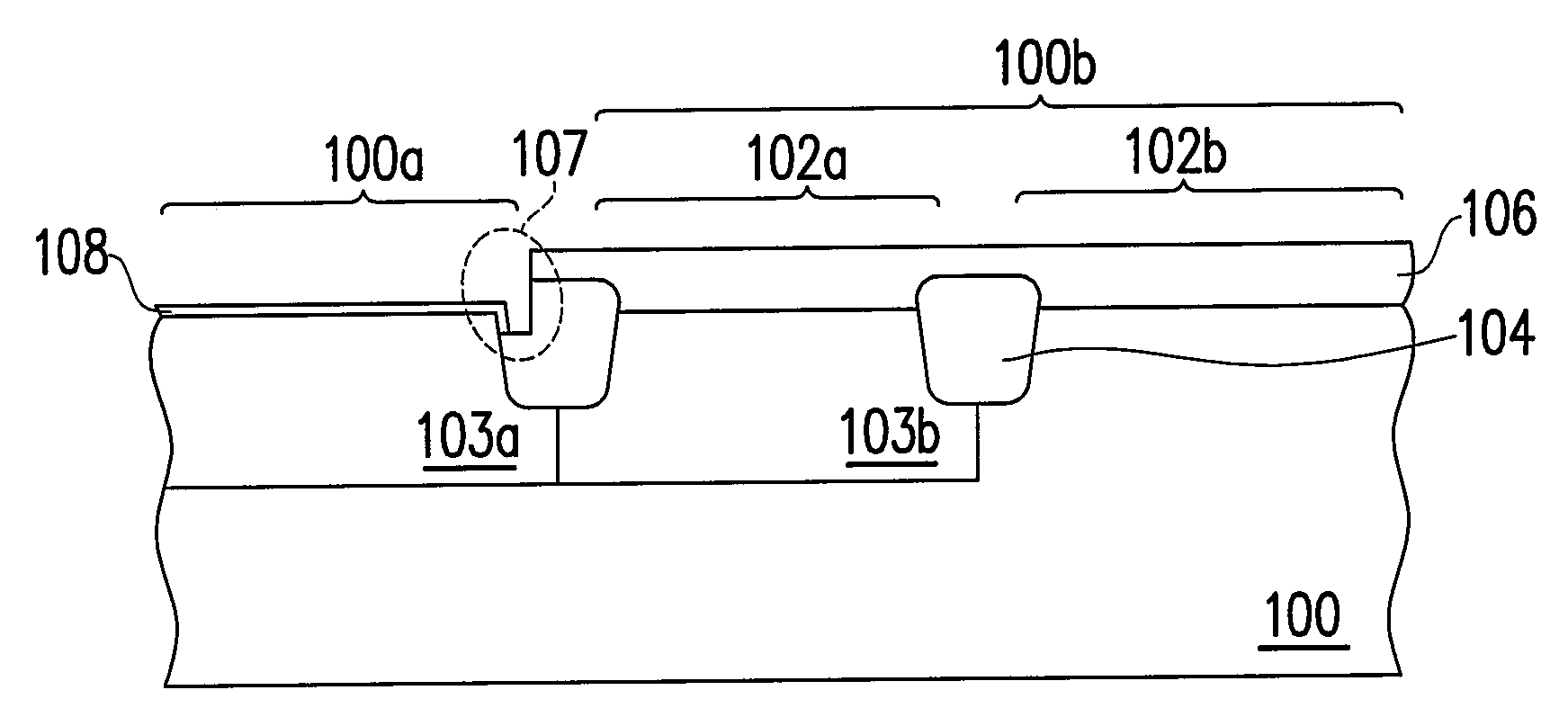
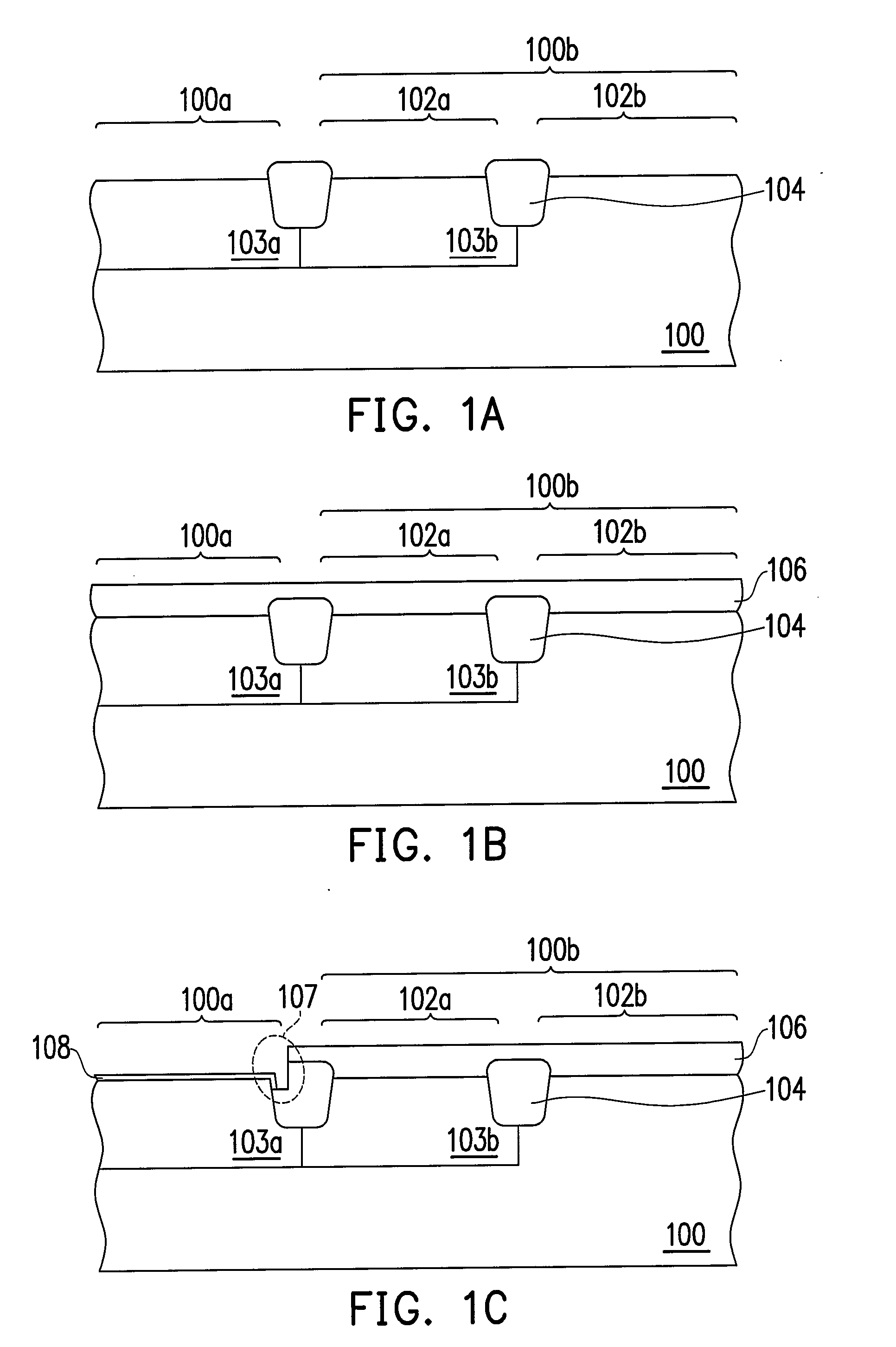
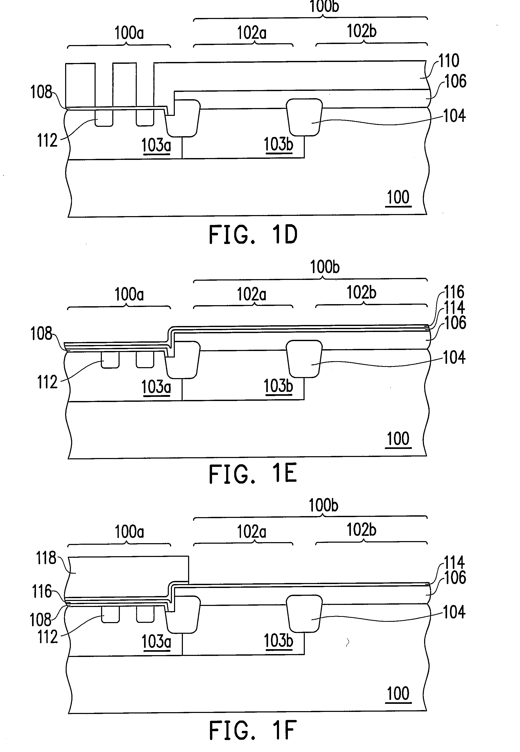
[0025]FIGS. 1A-1H are cross-sectional views showing selected process steps for fabricating a memory comprising a memory array area and a corresponding peripheral circuit area in accordance to one embodiment of the invention.

[0026]Referring to FIG. 1A, a semiconductor substrate 100 is provided. The semiconductor substrate 100 may be a silicon wafer, for example. The surface of the semiconductor substrate 100 is divided into at least a memory array area 100a and a peripheral circuit area 100b formed adjacent to each other. The peripheral circuit area 100b may further divide into at least a high voltage device region (HV) 102a and a low voltage device region (LV) 102b. Additionally, wells 103a, 103b may also form in the memory array area 100a and the high voltage device region (HV) 102a, respectively. The wells 103a, 103b are formed by implanting dopants in the substrate 100, for example. The wells may be either an N-well for forming PMOS devices or P-well for forming NMOS devices. Fur...


PUM


Abstract

A method for fabrication a memory having a memory area and a peripheral area includes forming a first gate insulating layer with a first thickness over a substrate of a first region in the peripheral area and a second insulating layer with a second thickness over the substrate of the memory region. Thereafter, a buried diffusion region is formed in the substrate of the memory area. A charge trapping layer and a third insulating layer are formed over the substrate. A gate insulating layer is formed in the second region in the peripheral area, wherein the first thickness is greater than a second thickness after removing the charge trapping layer and third insulating layer on the first and second region in the peripheral area. A conductive layer is formed over the substrate of the memory area and the peripheral area substantially after the gate insulating layer is formed.

Description

BACKGROUND OF THE INVENTION[0001]1. Field of Invention[0002]The present invention relates to a method for fabricating a semiconductor device. More particularly, the present invention relates to a method for fabricating a non-volatile memory.[0003]2. Description of Related Art[0004]As the integration of semiconductor devices increases, the line width of the semiconductor devices must be reduced. However, as the size of the semiconductor devices, for example, memory devices decreases, a variety of problems is resulted. For example, as the line width of a memory device is reduced, the channel length between the source and the drain is correspondingly reduced, leading to the short channel effect.[0005]Normally, a memory device integrates the memory cell arrays and the peripheral circuit elements onto a single chip. The peripheral circuit elements include high voltage (HV) devices and (LV) low voltage devices. The prior art method in forming such a memory device involves first forming a ...

Claims


Application Information

Patent Timeline
Patent Type & Authority Applications(United States)
IPC IPC(8): H01L21/8238H01L21/336H01L21/8242
CPCH01L21/823462H01L27/11573H01L27/11568H01L27/105H10B43/30H10B43/40
Inventor SHIH, YEN-HAOLAI, ERH-KUN
Owner MACRONIX INT CO LTD
Why Eureka
Try Eureka