Method for fabricating semiconductor device

a semiconductor and device technology, applied in the direction of semiconductor devices, basic electric elements, electrical appliances, etc., can solve the problems of affecting the size affecting the device characteristics of the memory, and acerbating the short channel effect, so as to prevent the expansion of the buried diffusion region and shorten the channel

Active Publication Date: 2008-01-24
MACRONIX INT CO LTD +1
View PDF3 Cites 13 Cited by
  • Summary
  • Abstract
  • Description
  • Claims
  • Application Information

AI Technical Summary

Benefits of technology

[0008]In view of the foregoing, the present invention provides a method for fabricating a memory in which the expansion of the buried diffusion region is prevented. Ultimately, the short channel effect is mitigated.

Problems solved by technology

Consequently, a variety of problems arise as the size of the cell of the memory device is miniaturized.
Accordingly, subsequent to the formation of the buried diffusion region in the semiconductor substrate, the high thermal budget processes, such as the fabrication process of the thick gate insulating layers for the high voltage devices, can seriously affect the size of the buried diffusion region.
Consequently, the short channel effect is acerbated and the device characteristics of the memory are difficult to control.
The inter-gate dielectric layer can potentially be damaged induced in other process steps.
Consequently, the quality of the device is compromised.

Method used


Image

  • Method for fabricating semiconductor device
  • Method for fabricating semiconductor device
  • Method for fabricating semiconductor device

Examples


Embodiment Construction

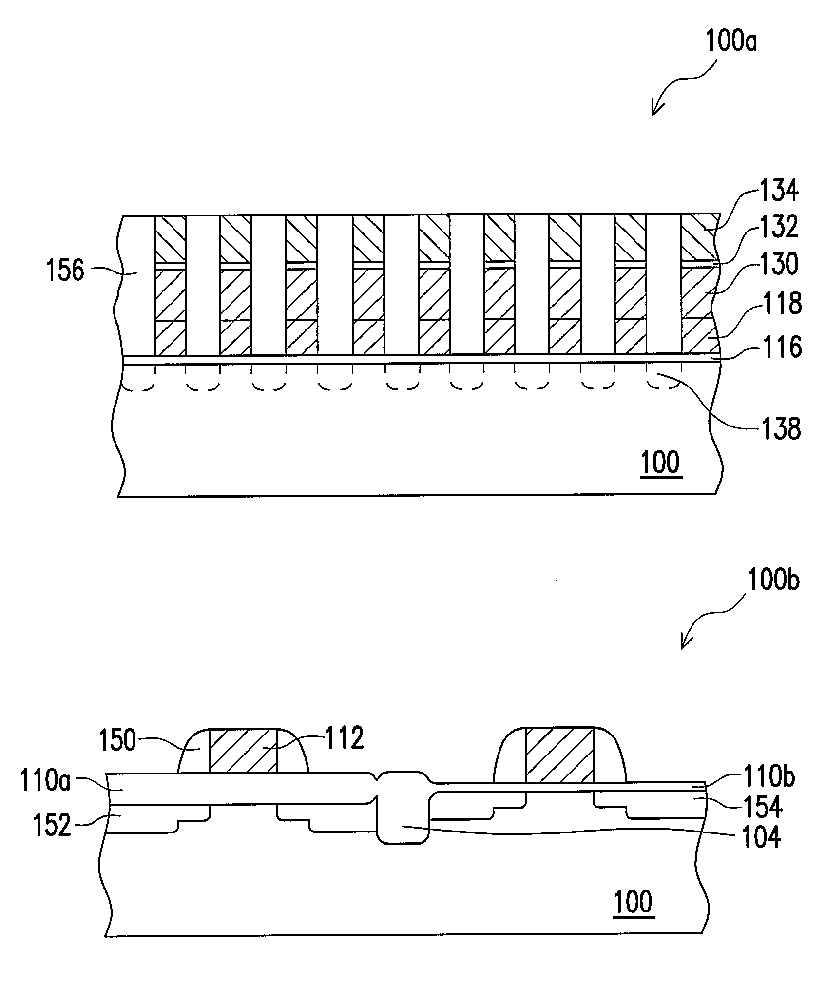
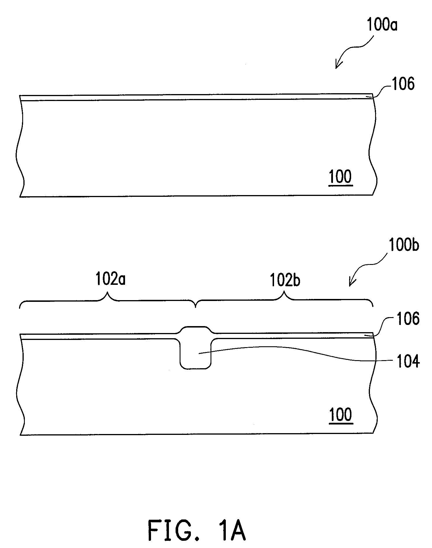
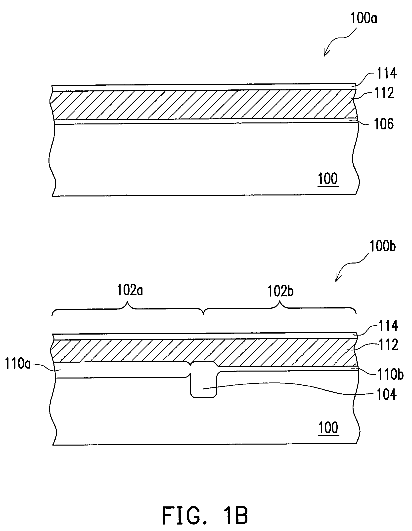
[0021]FIGS. 1A-1L and 1E′-1H′ are cross-sectional views showing selected process steps for fabricating a memory comprising a memory array area and a corresponding periphery circuit area in accordance to one embodiment of the invention. FIGS. 1E′-1H′ are cross-sectional views of the memory array area observed from a perpendicular direction from the viewing angle of FIGS. 1E-1H, respectively. Referring to FIG. 1A, a semiconductor substrate 100 is provided. The semiconductor substrate 100 may be a silicon wafer, for example. The surface of the semiconductor substrate 100 is divided into at least a memory array area 100a and a periphery circuit area 100b formed adjacent to the memory array area 100a. The periphery circuit area 100b, for example, a logic circuit area, may further divide into a high voltage transistor region (HV) 102a and a low voltage transistor region (LV) 102b. Additionally, the memory array area 100a may form within a cell well (not shown), while the high voltage tran...


PUM


Abstract

A method for fabrication a memory having a memory area and a periphery area is provided. The method includes forming a gate insulating layer over a substrate in the periphery area. Thereafter, a first conductive layer is formed in the memory area, followed by forming a buried diffusion region in the substrate adjacent to the sides of the first conductive layer. An inter-gate dielectric layer is then formed over the first conductive layer followed by forming a second conductive layer over the inter-gate dielectric layer. A transistor gate is subsequently formed over the gate insulating layer in the periphery area.

Description

BACKGROUND OF THE INVENTION[0001]1. Field of Invention[0002]The present invention relates to a method for fabricating a semiconductor device. More particularly, the present invention relates to a method for fabricating a memory having a memory area and a periphery area.[0003]2. Description of Related Art[0004]As the development of semiconductor technology advances for increasing the integration of semiconductor devices, the line width of the semiconductor devices must be reduced. Consequently, a variety of problems arise as the size of the cell of the memory device is miniaturized. For example, as the line width of the memory device reduced, the channel length between the source and the drain is correspondingly reduced leading to a short channel effect. The short channel effect is a result of the reduction in the threshold voltage and the increase in the sub-threshold current.[0005]Conventionally, a memory involves integrating memory cell arrays and logic circuit elements onto a sin...

Claims


Application Information

Patent Timeline
Patent Type & Authority Applications(United States)
IPC IPC(8): H01L21/8234
CPCH01L27/115H01L27/11546H01L27/11526H01L27/105H10B41/49H10B41/40H10B69/00
Inventor LO, CHUN-YUANWU, CHUN-PEI
Owner MACRONIX INT CO LTD
Why Eureka
Try Eureka