Production Method for Stacked Device

a production method and stacking technology, applied in the field of producing devices, can solve the problems of reducing yield rate and difficulty in handling semiconductor wafers, and achieve the effects of improving productivity and yield ratio, smooth cutting, and easy and smooth cutting

Inactive Publication Date: 2008-03-13
DISCO CORP
View PDF5 Cites 18 Cited by
  • Summary
  • Abstract
  • Description
  • Claims
  • Application Information

AI Technical Summary

Benefits of technology

[0010]In one aspect of the production method, only the rear surface of the device forming region of the wafer before the dividing process for dividing the wafer into the semiconductor chips is thinned by the grinding, and the initial thickness of the wafer is maintained on the peripheral extra region around the device forming region and the ring-shaped protrusion is thereby formed. Therefore, the wafer is thinned, but the rigidity of the wafer is ensured by the ring-shaped protrusion. Therefore, movement of the wafer to the etching process for forming the rear surface electrode portion by projecting the via electrode from the rear surface of the wafer and the etching process can be easily and smoothly performed. The movement of the wafer to the dividing process after the process can be safely performed without breaking the wafer. As a result, productivity and yield ratio can be improved.
[0011]According to a preferred embodiment of the present invention, the dividing process is performed while the rear surface of the wafer is exposed and held. According to a preferred embodiment of the present invention, the dividing process is performed after removing the ring-shaped protrusion on the peripheral extra region when the wafer is divided into plural devices by dicing the wafer by a cutting blade. Therefore, the wafer can be smoothly cut without the cutting blade interfering with the ring-shaped protrusion.
[0012]As is explained above, according to the present invention, the thinning of the wafer by grinding the rear surface is performed only at the region corresponding to the device forming region and the thick ring-shaped protrusion is formed on the peripheral extra region therearound, so that rigidity of the wafer can be obtained. As a result, the thinned semiconductor wafer can be easily handled and can be smoothly moved between processes, so that productivity and yield rate can be improved.

Problems solved by technology

However, since the semiconductor wafer is processed to be very thin in the above manner so as to be compact and thin, it is difficult to handle the semiconductor wafer when moving it to an etching process after it has thinned and when moving it to a dividing process after the etching process.
In addition, since the semiconductor wafer is easily broken, yield rate decreases.

Method used


Image

  • Production Method for Stacked Device
  • Production Method for Stacked Device
  • Production Method for Stacked Device

Examples


Embodiment Construction

[0026]One embodiment of a production method for semiconductor chips using the present invention will be explained hereinafter with reference to the drawings.

1. Semiconductor Wafer

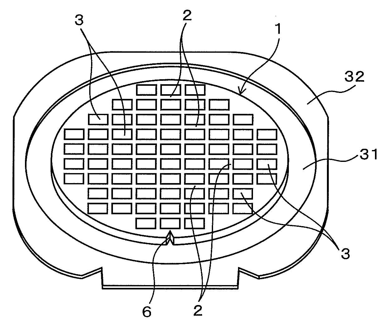
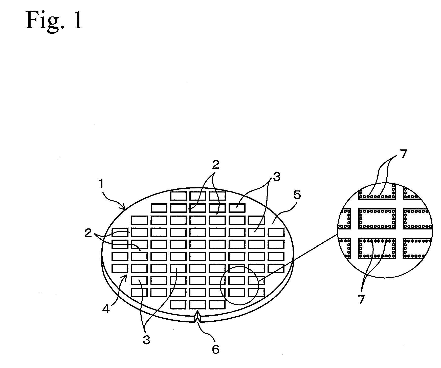
[0027]Reference numeral 1 in FIG. 1 denotes a disc-shaped semiconductor wafer (hereinafter referred to simply as a “wafer”) which is a material for producing semiconductor chips. For example, the wafer 1 is a silicon wafer having a thickness of about 600 μm. Plural rectangular semiconductor chips 3 (devices) are partitioned on the surface of the wafer 1 by grid-like predetermined division lines 2. An electronic circuit such as an IC (Integrated Circuit) or LSI (Large-Scale Integration) is formed on each surface of the semiconductor chips 3.

[0028]The plural semiconductor chips 3 are formed on a device forming region 4 having an approximately circular-shape which is concentric with the wafer 1. The device forming region 4 occupies most of the wafer. A ring-shaped peripheral extra region 5 on which the semicon...


PUM

PropertyMeasurementUnit
thicknessaaaaaaaaaa
heightsaaaaaaaaaa
thicknessaaaaaaaaaa

Abstract

A production method for obtaining a stacked device from a wafer is provided. The wafer has: a device forming region formed on a surface having plural devices formed thereon, the devices having surfaces and thicknesses; a peripheral extra region surrounding the device forming region; and plural metal electrodes embedded in the surfaces of the devices and having thicknesses which are equal to or larger than the thicknesses of the devices. The method includes: a protective tape applying process for applying a protective tape to the surface of the wafer; a rear surface recess forming process for thinning only a region, which corresponds to the device forming region, on a rear surface by grinding, thereby forming a recess on the rear surface, forming a ring-shaped protrusion projecting from the rear surface on the peripheral extra region, and exposing the metal electrodes at the rear surface; an etching process for removing mechanical damage, which is provided to the recess by the grinding, by etching to the recess, and forming a rear surface side electrode portion by projecting the exposed metal electrodes from a bottom surface of the recess; and a dividing process for dividing the wafer into the devices.

Description

[0001]This application claims priority under 35 U.S.C. § 119 to Japanese Patent Application No. JP2006-248383 filed Sep. 13, 2006, the entire content of which is hereby incorporated by reference.BACKGROUND OF THE INVENTION[0002]1. Field of the Invention[0003]The present invention relates to a method for producing devices (for example, semiconductor chips) from a semiconductor wafer (for example, silicon wafer), in which the device has a metal electrode penetrating the device.[0004]2. Description of Related Art[0005]In recent techniques for semiconductor devices, a stacked semiconductor package (for example, a multi-chip package (MCP) and a system-in-package (SIP)) having plural stacked semiconductor chips is effectively used in order to have a high density and be compact and thin. For example, a production method for the semiconductor package is a method in which semiconductor chips are stacked on a package substrate which is called an “interposer”, electrodes of the interposer and ...

Claims


Application Information

Patent Timeline
Patent Type & Authority Applications(United States)
IPC IPC(8): H01L21/78
CPCB23K26/03B23K26/032H01L21/78B23K26/0853B23K26/4075B23K26/034B23K26/40B23K2103/50
Inventor BROWN, MARK
Owner DISCO CORP
Why Eureka
Try Eureka