Writing error diagnosis method for charged particle beam photolithography apparatus and charged particle beam photolithography apparatus

a technology of photolithography and charge beam, which is applied in the field of writing error diagnosis method of charged particle beam photolithography apparatus, can solve problems such as pattern writing error, pattern design error, and pattern design error, and achieve the effect of avoiding pattern writing error

Active Publication Date: 2008-03-20
NUFLARE TECH INC
View PDF3 Cites 13 Cited by
  • Summary
  • Abstract
  • Description
  • Claims
  • Application Information

AI Technical Summary

Benefits of technology

[0015]According to the embodiments of the present invention, a writing error diagnosis method for a charged beam photolithography apparatus and a charged beam photolithography apparatus, which can specify an error cause (error occurrence state) within a short period of time when a pattern writing error occurs.

Problems solved by technology

This is because, once a pattern writing error occurs, not only the mask with the error cannot be used but also production of masks is stopped until a cause of writing error is specified and a countermeasure against the pattern writing error is made, thereby resulting in tremendous damage.
A pattern writing error (pattern error) is a phenomenon in which a pattern designed by a user cannot be exactly written on a target object.
As one of main causes of writing error, abnormal processing in a pattern writing circuit is known.
More specifically, in the abnormal processing, a normal output (processing result) cannot be obtained from a pattern writing circuit due to a defect, a defective operation, or the like in a circuit board or an element which constitutes the pattern writing circuit.
Essentially, even though a pattern writing error occurs in a prior art, there is no effective means for easily recognizing apparatus states when a pattern writing error occurs, i.e., writing data, a pattern writing condition, a writing pattern.
As a result, time is consumed to specify a cause of error.

Method used


Image

  • Writing error diagnosis method for charged particle beam photolithography apparatus and charged particle beam photolithography apparatus
  • Writing error diagnosis method for charged particle beam photolithography apparatus and charged particle beam photolithography apparatus
  • Writing error diagnosis method for charged particle beam photolithography apparatus and charged particle beam photolithography apparatus

Examples


first embodiment

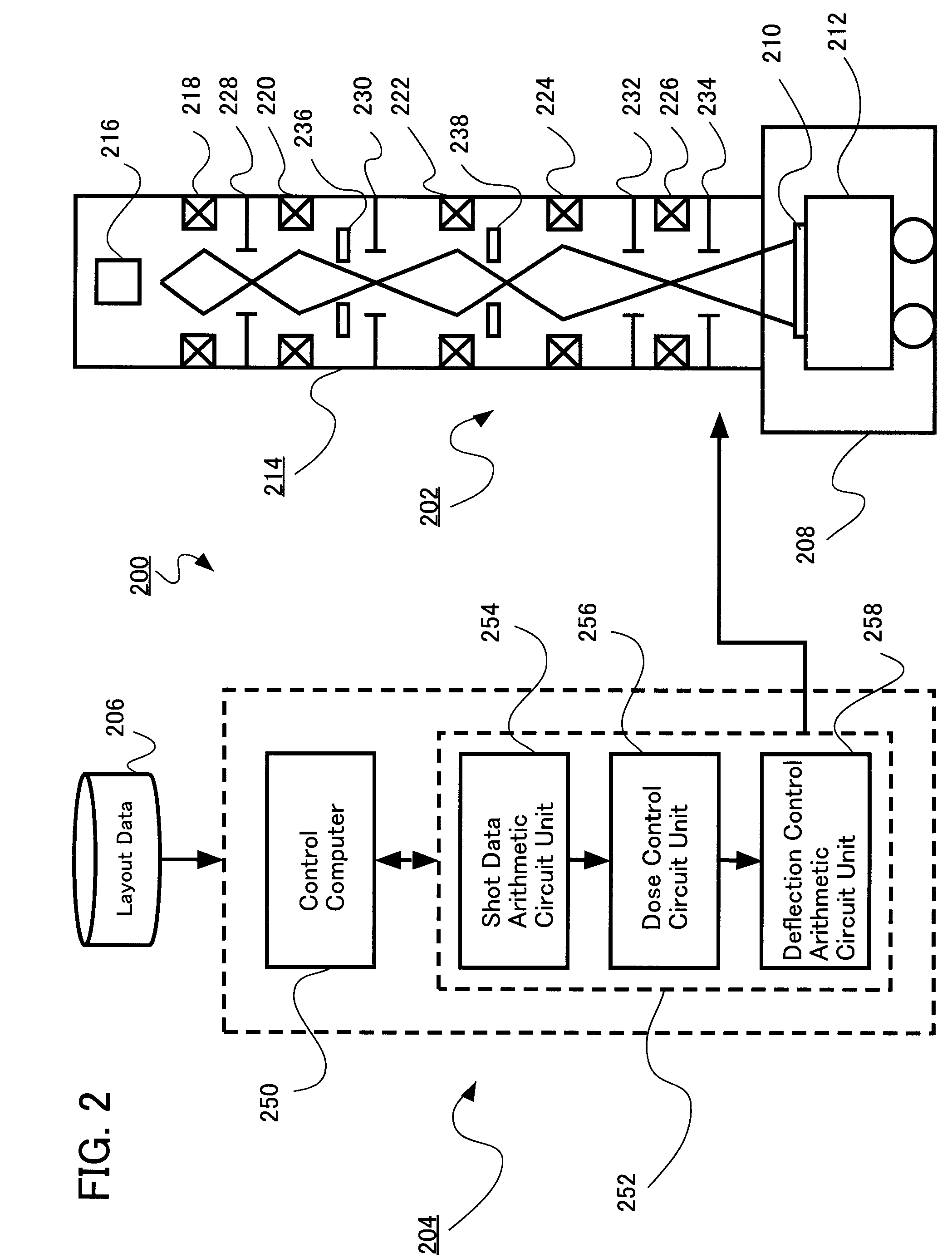
[0024]FIG. 2 is a schematic block diagram of an electron beam photolithography apparatus according to a first embodiment. An electron beam photolithography apparatus 200 is constituted by a pattern writing unit 202 and a writing control unit 204 which controls a pattern writing operation of the pattern writing unit 202. Layout data 206 (design data) of a semiconductor integrated circuit to be drawn is input and stored in advance in the electron beam photolithography apparatus 200.

[0025]In the pattern writing unit 202, a stage 212 on which a target object 210 such as a mask is placed is accommodated in a target object chamber 208. The stage 212 is driven in an X direction (left and right directions on the paper) and a Y direction (back and forth directions on the paper) by the writing control unit 204.

[0026]An electron beam optical system 214 is arranged above the target object chamber 208. The electron beam optical system 214 is constituted by an electron gun assembly 216, various l...

second embodiment

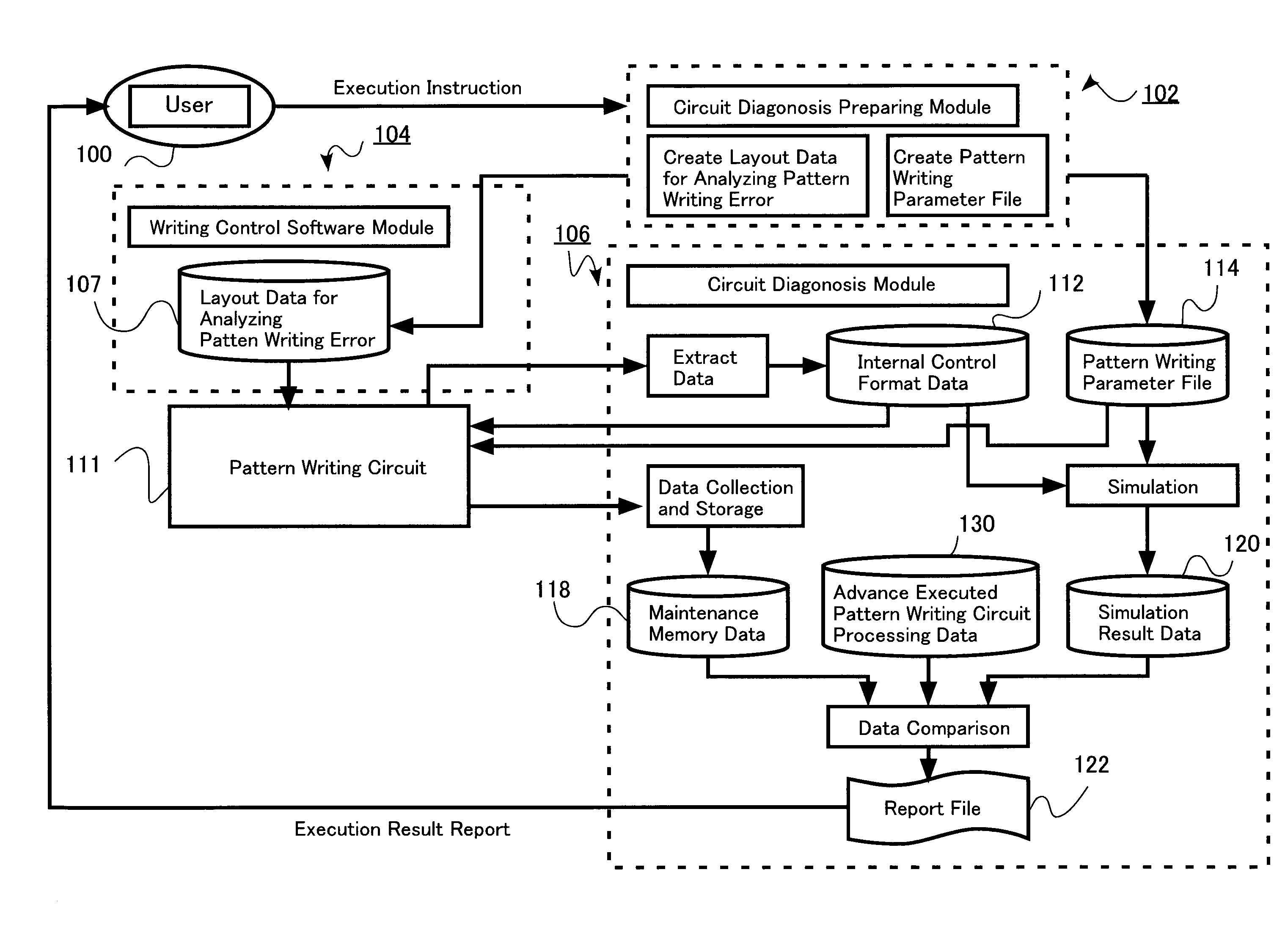
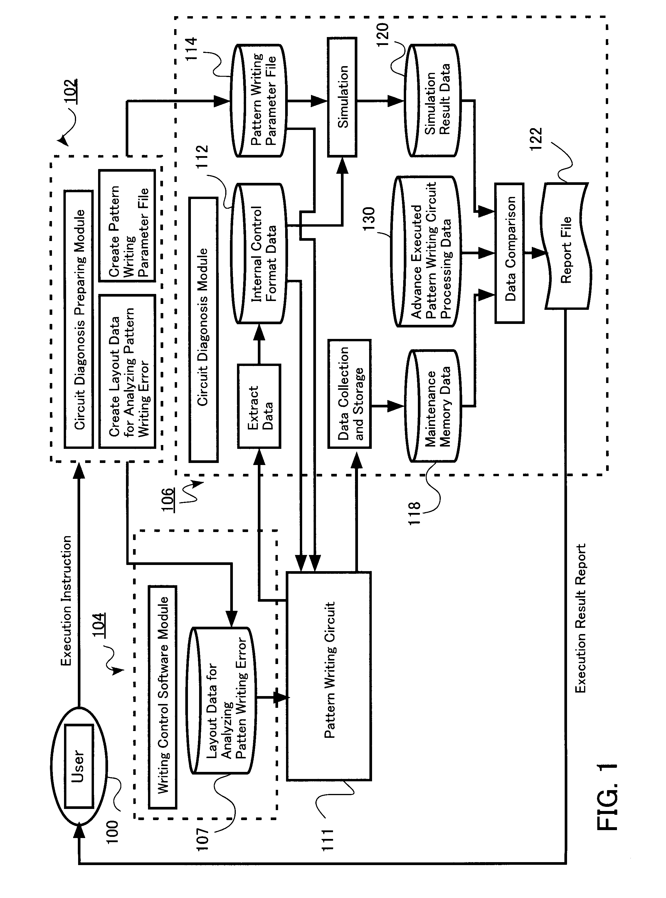
[0073]A second embodiment of the present invention will be described below. The second embodiment is the same as the first embodiment except that maintenance memory data which reproduces a collected state in which a pattern writing error occurs is compared with processing result data (also called advance executed pattern writing circuit processing result data) 130 (FIG. 1) of a pattern writing circuit obtained by executing a pattern writing process in advance as a correct data not the simulation result data 120 (FIG. 1) as correct data. The same description will be omitted.

[0074]FIG. 6 is a diagram for explaining operation steps of a circuit diagnosis module 106 according to the embodiment. Since the operation steps up to the step (S512) of collecting the maintenance memory data 118 are the same as those in the first embodiment, a description thereof will be omitted. After the collection of maintenance memory data (S512), the circuit diagnosis module 106 urges a user to select advan...


PUM


Abstract

A writing error diagnosis method for a charged beam photolithography apparatus and a charged beam photolithography apparatus which can specify an error cause within a short period of time in occurrence of a pattern writing error are provided. The writing error diagnosis method for a charged beam photolithography apparatus is a writing error diagnosis method for a charged beam photolithography apparatus which irradiates a charged beam on a target object to write a desired pattern. Processing result data of a pattern writing circuit at a position where a pattern writing error occurs is collected after the pattern writing error occurs, and the collected processing result data of the pattern writing circuit is compared with correct data. The charged beam photolithography apparatus has means which realizes the diagnosis method.

Description

CROSS-REFERENCE TO RELATED APPLICATION[0001]This application is based upon and claims the benefit of priority from the Japanese Patent Application No. 2006-150385, filed on May 30, 2006, the entire contents of which are incorporated herein by reference.FIELD OF THE INVENTION[0002]The present invention relates to a charged particle beam photolithography apparatus which writes a pattern of an LSI or the like on a target object such as a mask or a wafer, and more particularly, to a writing error diagnosis method for a charged particle beam photolithography apparatus and a charged particle beam photolithography apparatus, which easily specify a cause of a pattern writing error in occurrence of the pattern writing error.BACKGROUND OF THE INVENTION[0003]A lithography technique which leads development of micropatterning of a semiconductor device is a very important and an only process which generates a pattern in semiconductor manufacturing processes. In recent years, with a high degree of...

Claims


Application Information

Patent Timeline
Patent Type & Authority Applications(United States)
IPC IPC(8): G21G5/00
CPCB82Y10/00H01J37/3174B82Y40/00
Inventor KIMURA, HAYATOHANDA, YUJINWAKE, SEIJIMATSUKAWA, TAKUYATSUCHIYA, SEIICHI
Owner NUFLARE TECH INC
Why Eureka
Try Eureka