

Display device and method for manufacturing the same
a technology of semiconductor devices and display devices, applied in semiconductor devices, basic electric elements, electrical apparatus, etc., can solve the problems of low difficult precise alignment, and difficult manufacturing, so as to reduce manufacturing costs, improve efficiency in the use of silicon wafers, and increase the effect of area
- Summary
- Abstract
- Description
- Claims
- Application Information
AI Technical Summary
Benefits of technology
Problems solved by technology
Method used
Image

Examples
embodiment mode 1
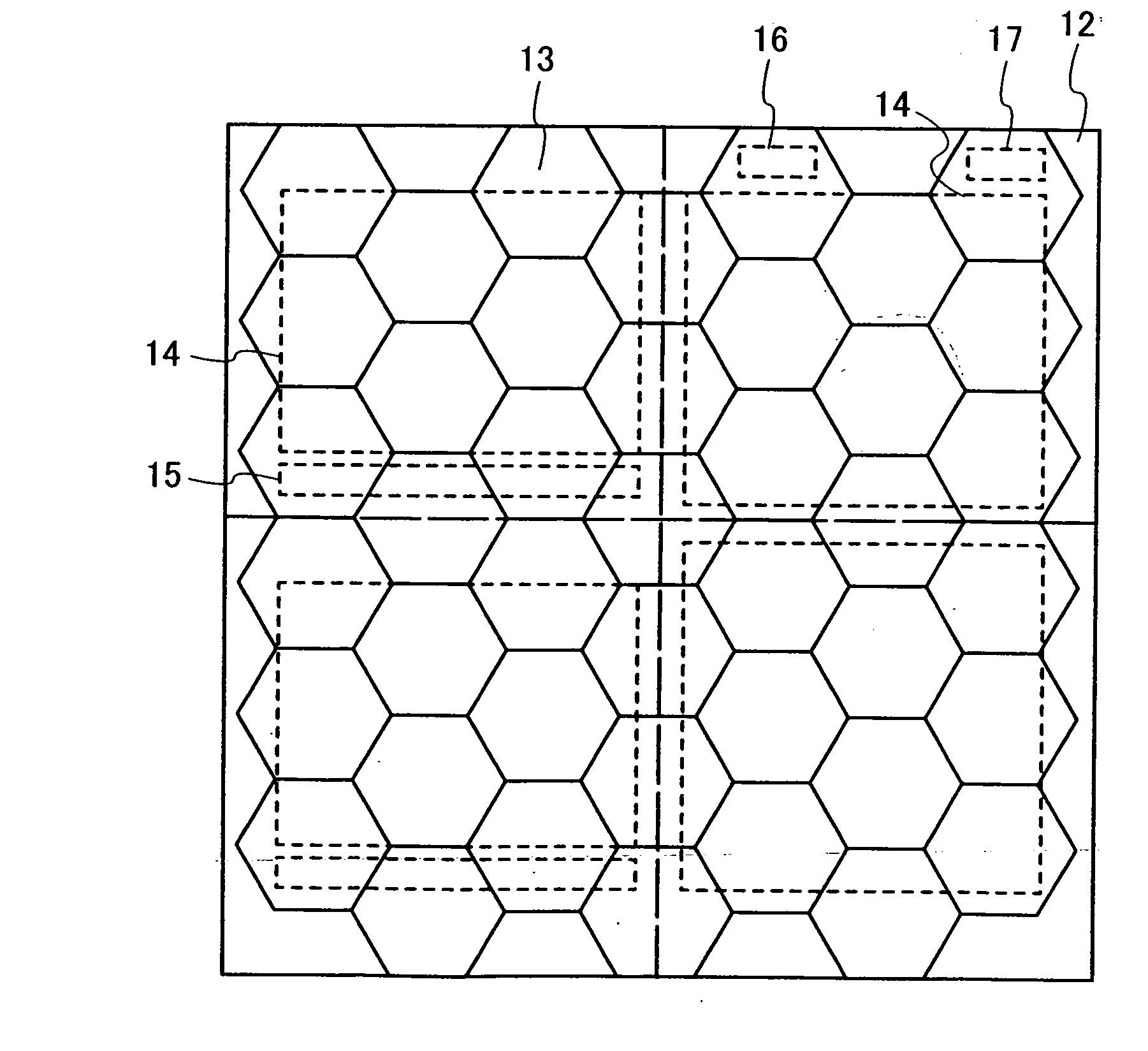
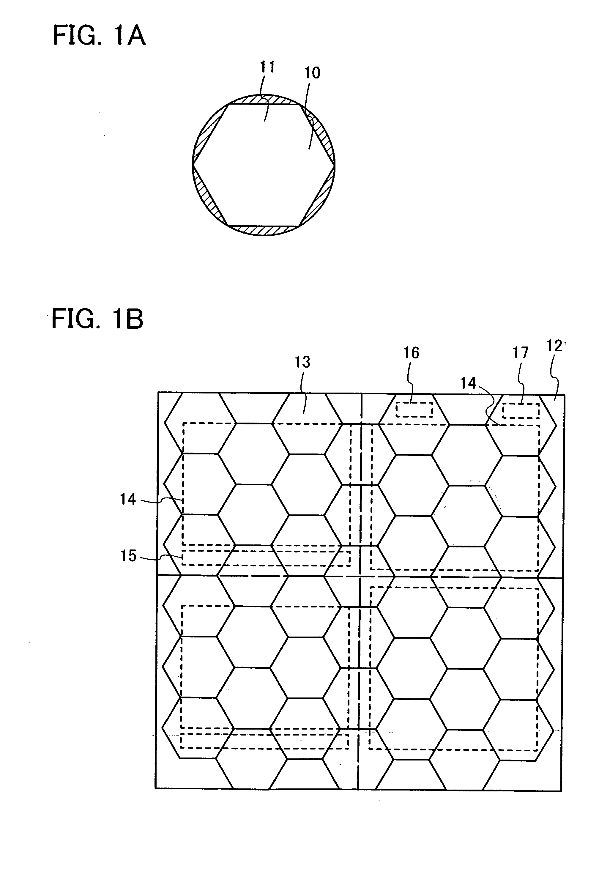
[0133]First, a specific method in which a circular silicon wafer is cut into a polygonal shape to be used for forming an SOI layer (a semiconductor layer) is described. As the polygonal shape to be cut out, a regular hexagon can be typically used. With a regular hexagon or a shape similar to the regular hexagon, SOI layers can be laid in a planer manner. In particular, the polygonal shape to be cut out is preferably a regular hexagon since a portion to be removed can be made small (see FIGS. 1A and 1B).
[0134]Note that in this specification, being “laid” refers to being arranged with a certain gap. For example, when SOI layers are arranged using a circular semiconductor substrate, a gap between the SOI layers includes a circumferential portion; thus, a space therebetween is not constant, and the SOI layers cannot be laid.
[0135]FIG. 1A illustrates a state in which a semiconductor substrate 10 such as a silicon wafer is cut into a regular hexagonal region 11. Regions of the semiconduct...
embodiment mode 2
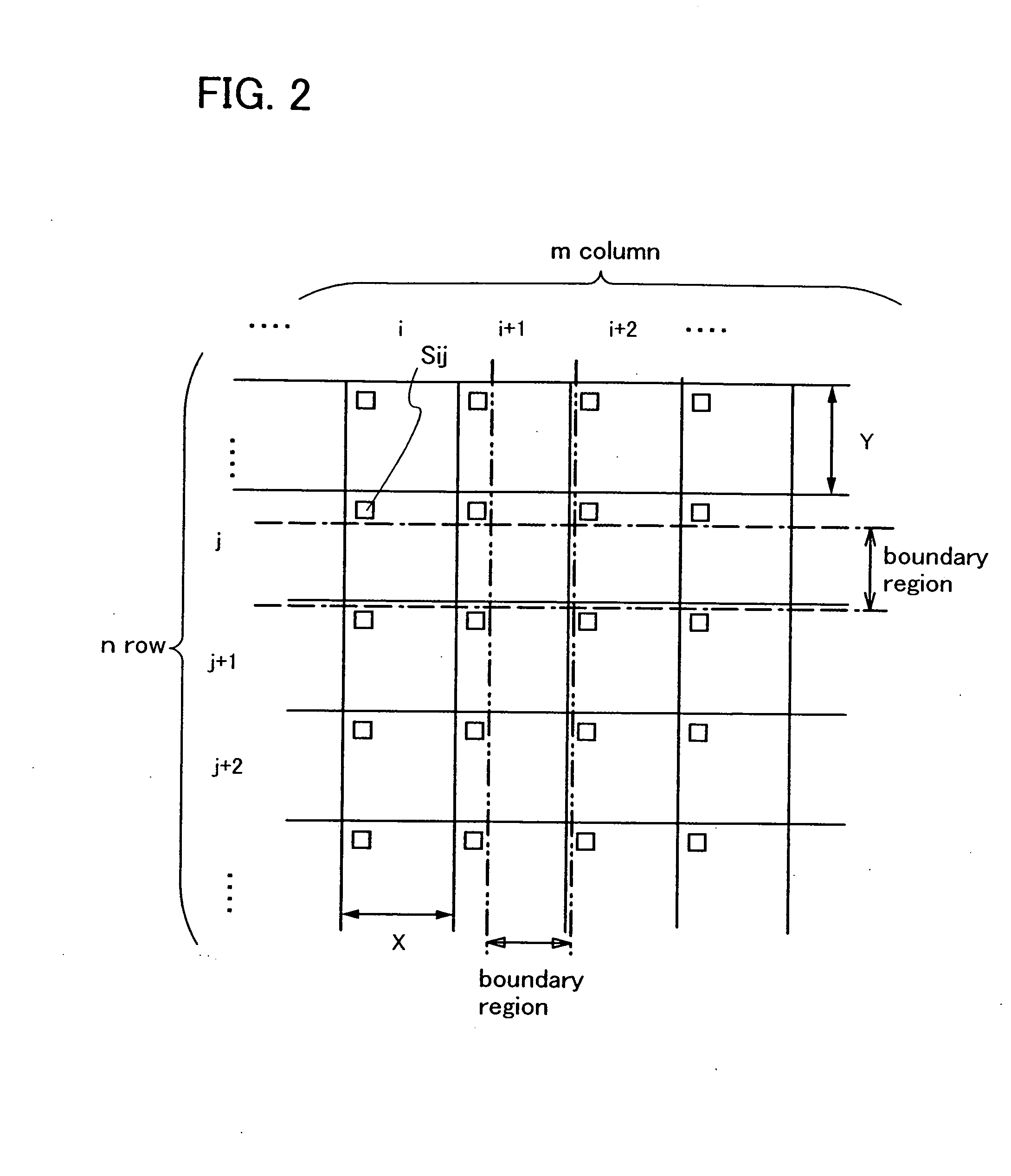
[0149]In this embodiment mode, effective arrangement of semiconductor regions included in the semiconductor device, which are formed by attaching and laying SOI layers as the example shown in Embodiment Mode 1, is described.
[0150]Since regular hexagonal SOI layers are laid in the example shown in Embodiment Mode 1, there is a boundary of SOI layers which has a slope that is not perpendicular or parallel to four sides of a substrate to which the SOI layers are attached (a large substrate such as a glass substrate, and hereinafter simply referred to as a large substrate). In such a case, when semiconductor regions included in the semiconductor device are arranged in accordance with the slope of the boundary, a possibility that a semiconductor region located at the boundary of SOI layers is used for a transistor can be reduced, and thus, yield of the semiconductor device can be improved.
[0151]Note that in this embodiment mode also, it is apparent that a shape of the SOI layer to be att...
embodiment mode 3
[0171]FIGS. 6A and 6B each show an SOI substrate according to the present invention. In FIG. 6A, a base substrate 9200 is a substrate having an insulating surface or an insulating substrate, and any of various glass substrates which are used in the electronics industry, such as an aluminosilicate glass substrate, an aluminoborosilicate glass substrate, and a barium borosilicate glass substrate, can be used. Alternatively, a quartz glass substrate or a semiconductor substrate such as a silicon wafer can be used. An SOI layer 9202 is a single-crystal semiconductor, and single-crystal silicon is typically used. Further alternatively, a crystalline semiconductor layer formed of silicon, germanium, or a compound semiconductor which can be separated from a single-crystal semiconductor substrate or a polycrystalline semiconductor substrate by a hydrogen ion implantation separation method can be used.
[0172]Between the base substrate 9200 and the SOI layer 9202 described above, a bonding lay...
PUM
 Abstract
Description
Claims
Application Information