ESD protection apparatus and circuit thereof

a protection apparatus and electronic static discharge technology, applied in the direction of circuit arrangement, semiconductor device details, semiconductor/solid-state device details, etc., can solve the problems of easy release of charges, damage to semiconductor chips, and the most undesirable mode of cdm, so as to improve electrical contact characteristics

Active Publication Date: 2008-03-20
HIMAX TECH LTD
View PDF5 Cites 116 Cited by
  • Summary
  • Abstract
  • Description
  • Claims
  • Application Information

AI Technical Summary

Benefits of technology

[0009]One aspect of the present invention discloses a layout pattern of an ESD protection circuit to protect semiconductor chips from the electro-static discharge, especially ones manufactured by high voltage processes. In one embodiment, an apparatus with a layout pattern for an ESD protection circuit comprises a first N type doped region; a first P type doped region coupled with the first N type doped region; a second N type doped region encompassed by a first N type WELL region; and the N type WELL region encompasses the first P type doped region. There may be a plurality of N type doped regions encompassed by the first P type doped region. The first N type doped region may be lightly doped. An N type heavily doped region may be positioned in the first N type doped region to improve electrical contact characteristics with electrodes.

Problems solved by technology

Transient voltages or currents brought by accumulated charges of certain materials can easily release charges due to friction.
Those charges will flow through the pins and cause damages to the semiconductor chips.
The CDM mode is the most undesirable mode for chips with large chip areas.
It can delay the response time for large transient voltages or currents which require a large junction area to pass through because larger area creates larger parasitic capacitance.
If the parasitic capacitor is too large, the protection mechanism of the ESD diode may not be able to react with those discharging events.

Method used


Image

  • ESD protection apparatus and circuit thereof
  • ESD protection apparatus and circuit thereof
  • ESD protection apparatus and circuit thereof

Examples


Embodiment Construction

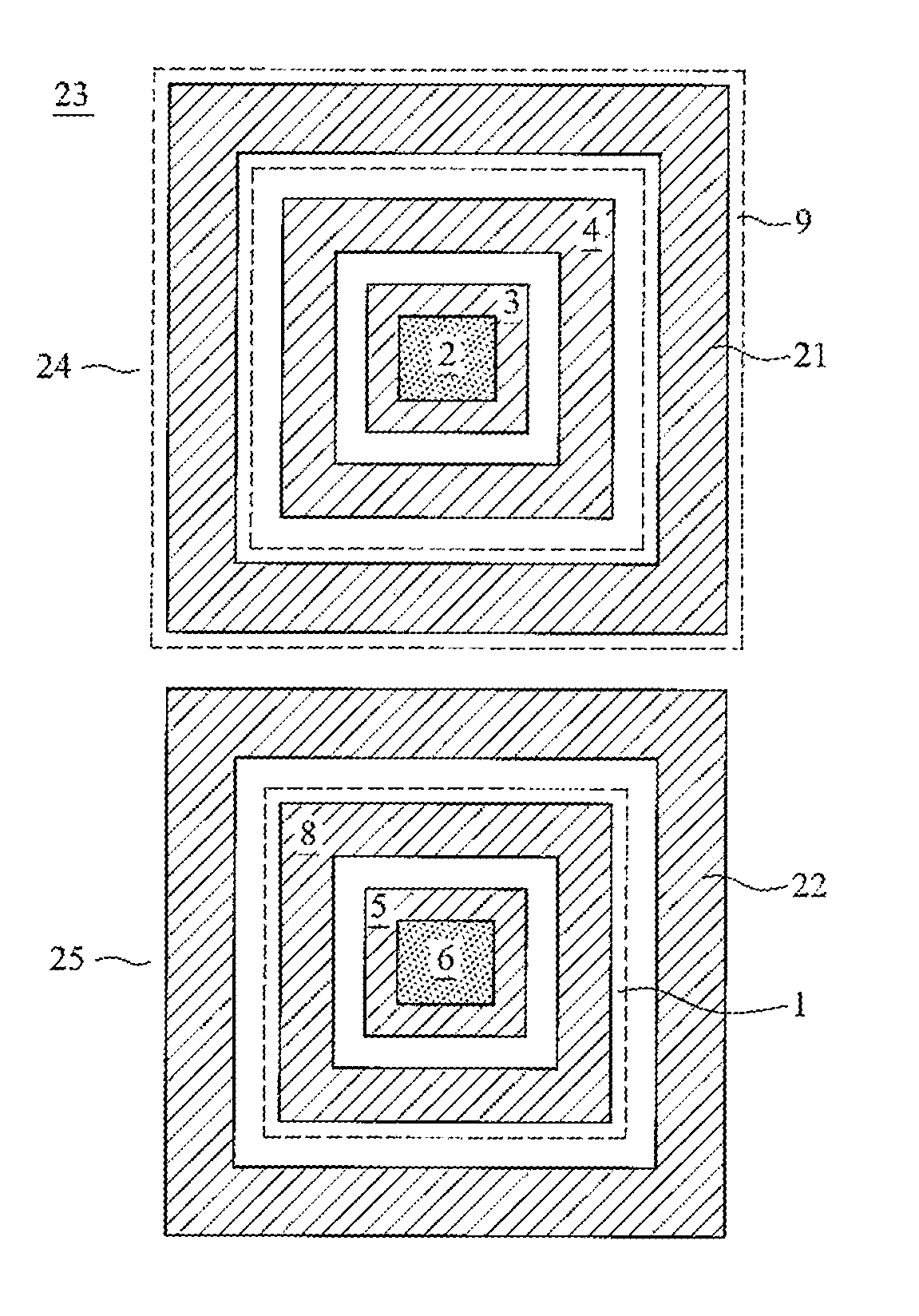
[0032]FIG. 2 shows layout patterns 23 of an ESD protection circuit on a substrate for high voltage applications. According to one embodiment of the present invention, a layout pattern 24 comprises an N type lightly doped region 3, a P type heavily doped region 4, and an N type WELL region 9 encompassing an N type heavily doped region 21. In one embodiment, the N type lightly doped region 3 is surrounded by two rings including the P type heavily doped region 4 and the N type heavily doped region 21. The N type lightly doped region 3 may encompass an N type heavily doped region 2 for connection to an electrode with better electrical properties.

[0033]The P type heavily doped region 4 may be entirely or partially replaced by a lightly doped region. The P type heavily doped region 4 connects to the substrate where the circuit components or the layout patterns are developed on. In this embodiment, the substrate may be a P type substrate. Similarly, the N type heavily doped region 21 may b...


PUM


Abstract

The present invention provides several embodiments with layout patterns for ESD protection. An apparatus with a layout pattern may be configured to protect I/O pads or the power rail. The layout pattern may designed to increase the current paths for ESD stress currents. For example, more rings may be applied. The present invention also provides circuit embodiments for ESD protection. According to one embodiment, an ESD protection circuit comprising four parasitic BJTs may be configured to protect the I/O pads or the power rail. More BJTs or resistors may be used to increase the current paths for ESD stress currents. Several variations and modifications may be made by changing the doping profiles of the doped regions.

Description

FIELD OF THE INVENTION[0001]The present invention relates to ESD (Electro Static Discharge) protection apparatuses, and more particularly, it relates to an ESD circuit and layout for the protection of other circuit components manufactured by a high voltage semiconductor process.BACKGROUND OF THE INVENTION[0002]ESD protection circuit is a component commonly found in almost every semiconductor chip. The ESD protection circuit protects a semiconductor chip from damages caused by transient voltages or currents. Transient voltages or currents brought by accumulated charges of certain materials can easily release charges due to friction. Therefore, ESD protection circuits are invented and positioned closely to pads in the chips. When excessive transient voltages or currents occur, ESD protection circuits can respond in time and direct the excessive transient voltages or currents into the power rails to avoid those voltages or currents from flowing to the core circuits.[0003]There are thre...

Claims


Application Information

Patent Timeline
Patent Type & Authority Applications(United States)
IPC IPC(8): H01L23/62
CPCH01L27/0259
Inventor CHEN, TUNG-YANG
Owner HIMAX TECH LTD
Why Eureka
Try Eureka