Light-emitting element having ZnO transparent electrode and method for manufacturing same

a technology light-emitting element, which is applied in the direction of crystal growth process, polycrystalline material growth, instruments, etc., can solve the problems of current leakage and efficiency drooping, light-emitting diode can become susceptible to electrostatic discharge, and ito layer has a thickness limit, so as to improve the electrical characteristics of light-emitting diodes, improve the production yield of zno transparent electrodes, and improve the electrical contact characteristics

Active Publication Date: 2019-09-10
SEOUL VIOSYS CO LTD
View PDF19 Cites 0 Cited by
  • Summary
  • Abstract
  • Description
  • Claims
  • Application Information

AI Technical Summary

Benefits of technology

[0043]According to exemplary embodiments, the light emitting diode employs the ZnO transparent electrode, which includes a ZnO seed layer and ae ZnO bulk layer formed by different processes and exhibits good electrical contact characteristics with the second conductivity type semiconductor layer, thereby improving electrical characteristics of the light emitting diode. In addition, the ZnO transparent electrode has a predetermined level or more of crystallinity to improve production yield of the ZnO transparent electrode and thus can be easily applied to mass production of light emitting diodes.
[0044]According to exemplary embodiments, the ZnO transparent electrode can secure sufficient current spreading in the light emitting diode, thereby enabling omission of a current blocking layer and improvement in resistance with respect to electrostatic discharge (ESD) while simplifying a manufacturing process. Further, the process of partially removing the second conductivity type semiconductor layer and the active layer to expose a portion of the first conductivity type semiconductor layer and the process of partially removing the ZnO transparent electrode in a predetermined pattern can be performed using the same mask. As a result, it is possible to simplify the manufacturing process while reducing manufacturing costs.
[0045]According to some exemplary embodiments, the light emitting diode employs both an ITO layer and a ZnO layer, thereby improving ohmic contact characteristics. Furthermore, the ZnO layer is formed to cover upper and side surfaces of the ITO layer, thereby improving light extraction efficiency.

Problems solved by technology

As a result, electric current is not effectively spread in the p-type semiconductor layer in the horizontal direction, thereby causing current crowding in a specific region of the semiconductor layer.
If current crowding occurs in the semiconductor layer, the light emitting diode can become susceptible to electrostatic discharge and can suffer from current leakage and efficiency drooping.
However, the ITO layer has a limit in thickness increase due to light absorptivity thereof.
These processes require separate masks for patterning, thereby providing process inconvenience and increasing manufacturing costs.
However, a transparent electrode using typical ZnO exhibits poor electrical characteristics and causes increase in forward voltage Vf when applied to a light emitting diode.
Moreover, typical ZnO has low production yield and thus is not suitable for mass production of light emitting diodes.

Method used


Image

  • Light-emitting element having ZnO transparent electrode and method for manufacturing same
  • Light-emitting element having ZnO transparent electrode and method for manufacturing same
  • Light-emitting element having ZnO transparent electrode and method for manufacturing same

Examples


Embodiment Construction

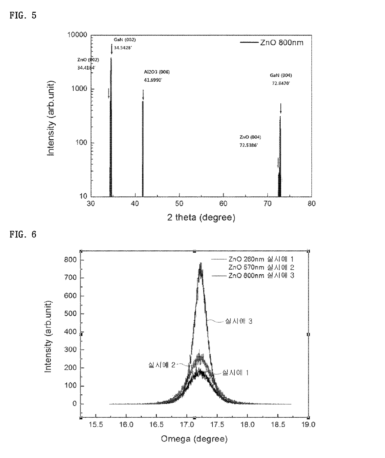
, the ZnO transparent electrodes 130 have thicknesses of 260 nm, 570 nm and 800 nm, respectively.

[0096]Referring to FIG. 6, as obtained by XRD ω scanning, the main peaks of the ZnO transparent electrode 130 of Example 1 may have a full width at half maximum of about 1,436 arc sec, the main peaks of the ZnO transparent electrode 130 of Example 2 may have a full width at half maximum of about 1,428 arc sec, and the main peaks of the ZnO transparent electrode 130 of Example 3 may have a full width at half maximum of about 869 arc sec. This result shows that, even when the thickness of the ZnO transparent electrode 130 increases from 260 nm to 570 nm, the full width at half maximum of the main peaks obtained by XRD ω scanning does not significantly decrease and crystallinity of the ZnO transparent electrode 130 does not significantly vary. On the contrary, when the thickness of the ZnO transparent electrode 130 increases from 570 nm to 800 nm, the full width at half maximum of the main ...


PUM

PropertyMeasurementUnit
thicknessaaaaaaaaaa
thicknessaaaaaaaaaa
thicknessaaaaaaaaaa

Abstract

A light-emitting electrode having a ZnO transparent electrode and a method for manufacturing the same are provided. A light-emitting element according to an embodiment comprises: a light-emitting structure comprising a first conductive semiconductor layer, an active layer, and a second conductive semiconductor layer; and a ZnO transparent electrode, which is positioned on the second conductive semiconductor layer, which makes an Ohmic contact with the second conductive semiconductor layer, and which comprises monocrystalline ZnO, wherein the diffraction angle of a peak of the ZnO transparent electrode, which results from X-ray diffraction (XRD) omega 2theta (ω2θ) scan, is in the range of ±1% with regard to the diffraction angle of a peak of the second conductive semiconductor layer, which results from XRD ω2θ scan, and the FWHM of a main peak of the ZnO transparent electrode, which results from XRD omega (ω) scan, is equal to or less than 900 arc sec.

Description

TECHNICAL FIELD[0001]Exemplary embodiments of the present disclosure relate to a light emitting diode and a method of manufacturing the same, and more particularly, to a light emitting diode including a ZnO transparent electrode and a method of manufacturing the same.BACKGROUND ART[0002]In a light emitting diode using nitride semiconductors, a p-type semiconductor layer has lower electrical conductivity than an n-type semiconductor layer. As a result, electric current is not effectively spread in the p-type semiconductor layer in the horizontal direction, thereby causing current crowding in a specific region of the semiconductor layer. If current crowding occurs in the semiconductor layer, the light emitting diode can become susceptible to electrostatic discharge and can suffer from current leakage and efficiency drooping.[0003]In general, an indium tin oxide (ITO) layer is used to provide current spreading in a p-type semiconductor layer. Since the ITO layer is optically transmissi...

Claims


Application Information

Patent Timeline
Patent Type & Authority Patents(United States)
IPC IPC(8): H01L33/42H01L33/32H01L33/62H01L33/10G02F1/1335H01L33/00C30B7/00C30B29/16H01L33/38
CPCH01L33/42G02F1/133603H01L33/10H01L33/325H01L33/62H01L2933/0016C30B29/16H01L33/007H01L33/32H01L33/387C30B7/005
Inventor LEE, JIN WOONGSHIN, CHAN SEOBLEE, KEUM JULEE, SEOM GEUNYANG, MYOUNG HAKRICHARDSON, JACOB J.O'HARA, EVAN C.
Owner SEOUL VIOSYS CO LTD
Why Eureka
Try Eureka