Semiconductor device and method of fabricating the same

a technology of semiconductor devices and semiconductors, applied in semiconductor devices, semiconductor/solid-state device details, electrical apparatus, etc., can solve the problems of affecting the reliability of devices, and tendency toward higher integration

Inactive Publication Date: 2016-09-13
SONY CORP
View PDF44 Cites 0 Cited by
  • Summary
  • Abstract
  • Description
  • Claims
  • Application Information

AI Technical Summary

Benefits of technology

[0017]An object of the present invention is to provide a semiconductor device with a high-reliability and a high-durability, which is capable of forming solder bumps on electrode pads made from a metal other than Al without degrading the adhesion strength between the electrode pads and the solder bumps and the electric contact characteristic therebetween, and to provide a method of fabricating the semiconductor device.
[0021]In the semiconductor device according to the first aspect of the present invention, since the adhesion layer is formed between the electrode pads and the barrier metal for increasing the adhesion therebetween, even if the electrode pads are changed from the convention Al based electrode pads into the Cu based electrode pads, it is possible to prevent degradation of the adhesion strength between the Cu based electrode pads and the solder bumps and the failure of the electric contact characteristic therebetween. That is to say, in order to keep up with the next-generation high speed LSIs adopting Cu based interconnections, the function of the barrier metal film having been used for improving the adhesion between electrode pads and solder bumps is reinforced by provision of the adhesion layer.
[0022]Accordingly, the solder ball bumps appropriate to the next-generation high speed LSI adopting the Cu interconnection layer can be formed, and since the barrier metal function is reinforced by adding the adhesion layer to the conventional barrier metal film, even if various heat-treatments are applied to the substrate after formation of the solder layer, it is possible to effectively prevent thermal diffusion of solder, and hence to obtain good electric contact characteristic between the finally formed solder bumps and the Cu based electrode pads and also increase the adhesion strength therebetween. This makes it possible to improve the reliability and durability of a device product on which the semiconductor chip is mounted by the flip-chip mounting method. In summary, according to the semiconductor device of the first aspect of the present invention, it is possible to improve the electric contact characteristic, reliability, and durability of a device product on which the next-generation high speed LSI chip adopting Cu interconnections is mounted by the flip-chip mounting method.
[0025]In the method of fabricating a semiconductor device according to the second aspect of the present invention, the passivation film is selectively etched using the resist film patterned into a specific shape as a mask to expose the electrode pads, and of the adhesion layer formed over the entire surface of the base, the unnecessary portion of the adhesion layer located on the resist film is removed together with the resist film by lifting-off the resist film, to allow only the portion of the adhesion layer located on the electrode pads to remain. That is to say, the resist film patterned into a specific shape is used for both the etching mask and the lift-off film. Accordingly, it is possible to eliminate the necessity for provision of the step of forming a resist film for forming the adhesion layer only on the electrode pads and the lithography step for patterning the resist film, and hence to effectively form the adhesion layer in self-alignment over the entire surfaces of the electrode pads exposed by selective etching of the passivation film without increasing the number of processing steps.
[0026]Accordingly, even if the electrode pads are changed from the Al based electrode pads into the Cu based electrode pads, the adhesion layer can be effectively formed in self-alignment on the entire surfaces of the Cu based electrode pads. This makes it possible to increase the adhesion between the Cu based electrode pads and the barrier metal film and hence to prevent the degradation of adhesion strength between the Cu based electrode pads and the solder bumps and the failure in electric contact characteristic therebetween. In summary, according to the method of fabricating the semiconductor device of the second aspect of the present invention, it is possible to improve the electric contact characteristic, reliability, and durability of a device product on which the next-generation high speed LSI chip adopting Cu interconnections is mounted by the flip-chip mounting method.
[0028]In this way, the semiconductor device and the fabrication method thereof according to the present invention is very useful to realize a semiconductor device designed on the basis of the fine design rule and required having high-integration, high-performance, and high-reliability.

Problems solved by technology

While Al has been used as an interconnection material of LSIs for a long time, the use of Al has come to cause serious problems associated with delay of signals or deterioration in the reliability in multiple interconnection layers along with tendency toward higher integration, finer-geometries, and higher operational speed of LSIs.
However, since the above-described process of forming solder ball bumps on electrode pads via a BLM film is predicated on the use of Al based electrode pads, if such a process is applied to an LSI using Cu electrode pads as terminals of Cu interconnections in place of the conventional Al based electrode pads as terminals of Al based interconnections, there may occur the following problem.
Namely, since the adhesion strength between the BLM film and the Cu electrode pads is lowered, there may easily arise the falling of solder ball bumps from a semiconductor chip upon mounting of the semiconductor chip on a printed wiring board or the failure in electric contact characteristic between the Cu electrode pads and the solder ball bumps when the semiconductor chip undergoes a temperature cycle or a high temperature load, thereby exerting adverse effect on the device reliability.

Method used


Image

  • Semiconductor device and method of fabricating the same
  • Semiconductor device and method of fabricating the same
  • Semiconductor device and method of fabricating the same

Examples


example 1

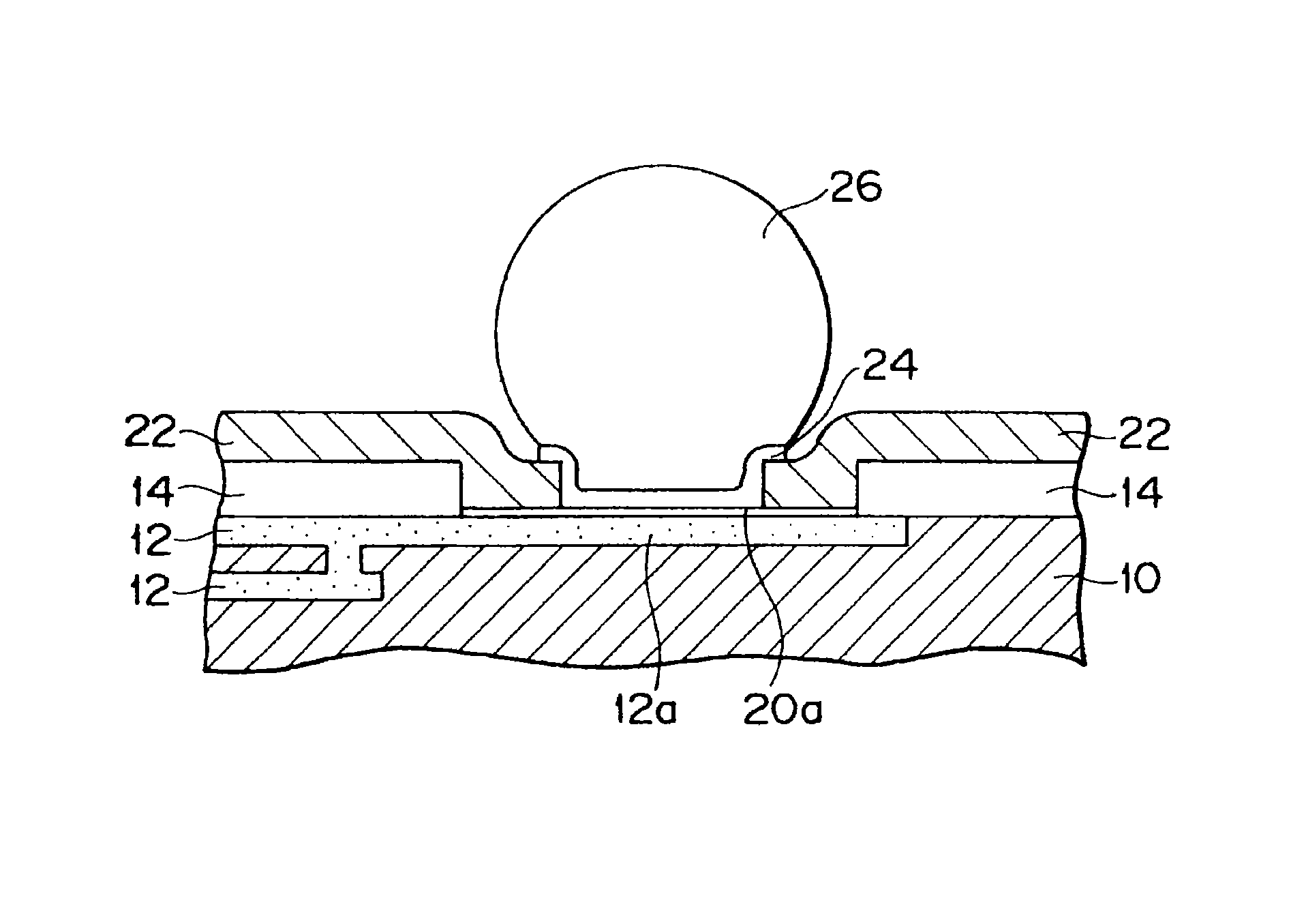
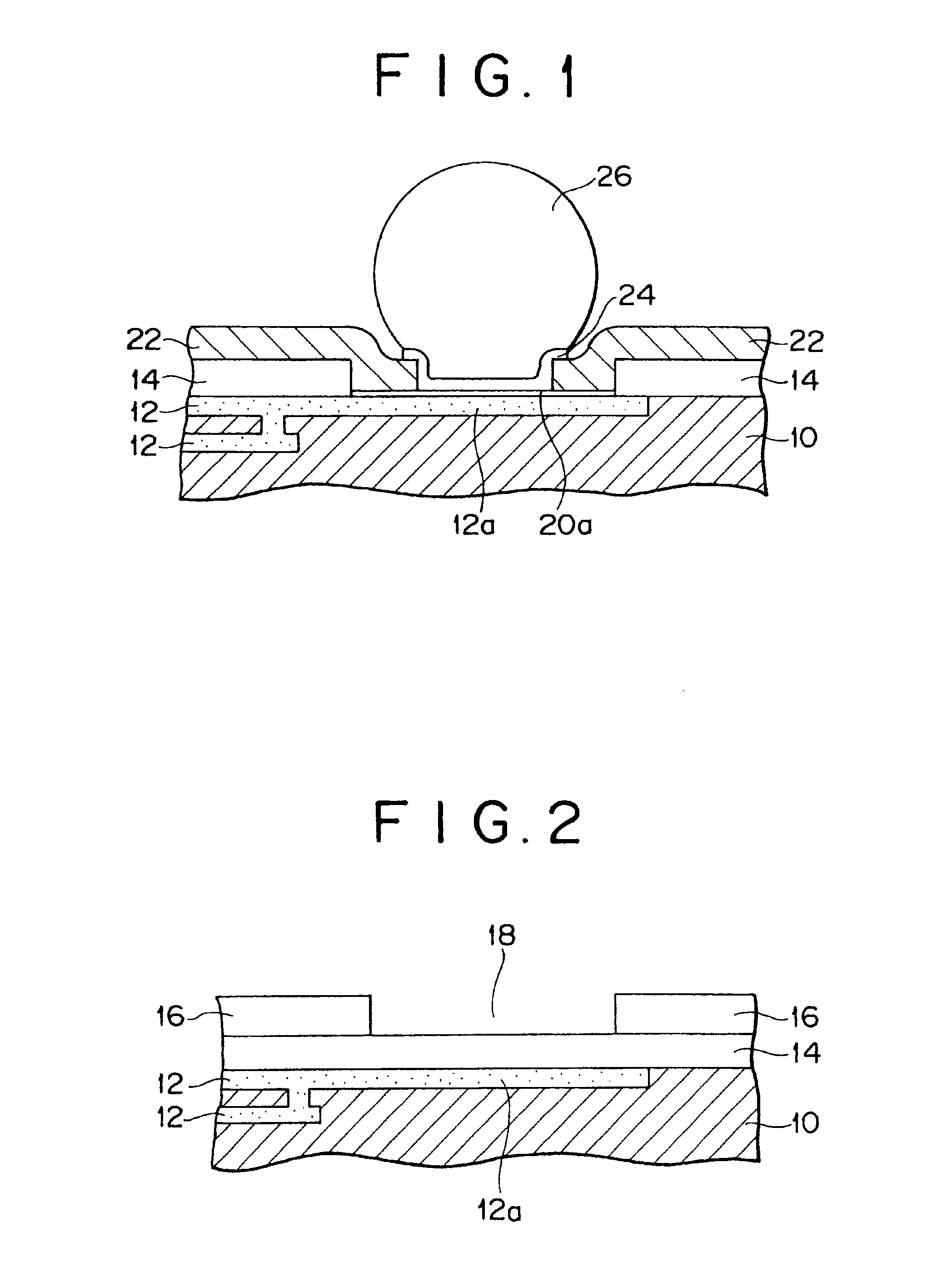
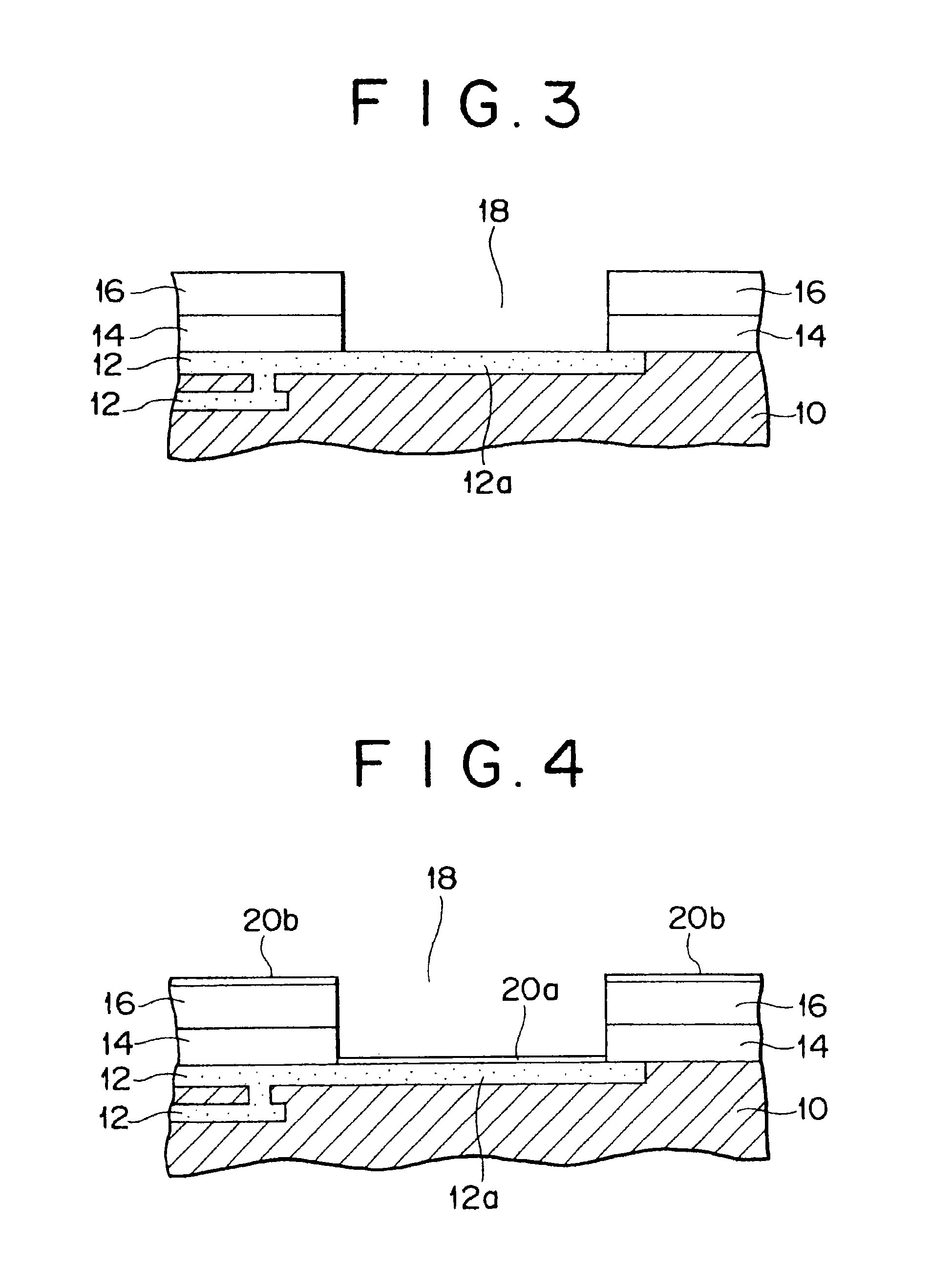
[0058]The selective etching of the silicon nitride film 14 with the resist film 16 taken as a mask was performed using the magnetron RIE apparatus under the following condition:[0059]flow rate of reactive gas: C4F8 / CO=10 / 90 sccm[0060]pressure: 2.0 Pa[0061]RF power: 2.2 W / cm2 [0062]strength of magnetic field: 150 Gauss

[0063]The formation of an Al film as the adhesive layers 20a and 20b was performed using a normal sputter apparatus under the following condition:[0064]DC power: 4.0 kW[0065]flow rate of atmospheric gas: Ar=100 sccm[0066]pressure: 0.5 Pa[0067]temperature of wafer stage: room temperature[0068]thickness of Al adhesion layer: 0.1 μm

[0069]The formation of each of films constituting the BLM film 24 having the stacked structure of Cr / Cu / Au was performed by a normal sputter apparatus under the following condition:

[0070](1) Formation Condition of Cr Film[0071]DC power: 3.0 kW[0072]flow rate of atmospheric gas: Ar=75 sccm[0073]pressure: 1.0 Pa[0074]temperature of wafer stage: 50...

example 2

[0088]The selective etching for the silicon nitride film 14 with the resist film 16 taken as a mask using the magnetron RIE apparatus under the following condition:[0089]flow rate of reactive gas: C4F8 / CO=10 / 90 sccm[0090]pressure: 2.0 Pa[0091]RF power: 2.2 W / cm2 [0092]strength of magnetic field: 150 Gauss

[0093]The formation of a Ti film as the adhesive layers 20a and 20b was performed using a normal sputter apparatus under the following condition:[0094]DC power: 5.0 kW[0095]flow rate of atmospheric gas: Ar=100 sccm[0096]pressure: 0.5 Pa[0097]temperature of wafer stage: room temperature[0098]thickness of Ti adhesion layer: 0.1 μm

[0099]The formation of each of films constituting the BLM film 24 having the stacked structure of Ti / Cu / Au was performed using a normal sputter apparatus under the following condition:

[0100](1) Formation Condition of Ti Film[0101]DC power: 4.0 kW[0102]flow rate of atmospheric gas: Ar=75 seem[0103]pressure: 1.0 Pa[0104]temperature of wafer stage: 50° C.[0105]t...


PUM

PropertyMeasurementUnit
adhesionaaaaaaaaaa
thicknessaaaaaaaaaa
densityaaaaaaaaaa

Abstract

An adhesion layer made from Al film or Ti film is formed on Cu electrode pad portions as external connection terminals of a Cu interconnection layer of an LSI formed on the surface layer of a semiconductor substrate. A BLM film having a stacked structure of Cr / Cu / Au or Ti / Cu / Au is formed on the adhesion layer. Solder ball bumps made from Pb and Sn are formed on the BLM film. The adhesion layer ensures a high adhesion strength and a high electric contact characteristic between the Cu electrode pad portions and the BLM film, that is, between the Cu electrode pads and the solder ball bumps.

Description

RELATED APPLICATION DATA[0001]The present application is a reissue application of application Ser. No. 09 / 313,172, now U.S. Pat. No. 6,545,355, issued Apr. 8, 2003, which claims priority to Japanese Application No. P10-141481 filed May 22, 1998, which application is incorporated herein by reference to the extent permitted by law.BACKGROUND OF THE INVENTION[0002]The present invention relates to a semiconductor device and a method of fabricating the semiconductor device, and particularly to a semiconductor device in which solder bumps are formed on electrode pads via a barrier metal film is and a method of fabricating the semiconductor device.[0003]To increasingly progress miniaturization of electronic equipment, it is important how improve the mounting density of electronic parts. With respect to semiconductor ICs (Integrated Circuits), studies have been actively made to develop such a high density mounting technology as to directly mount a bare chip on a printed wiring board, typica...

Claims


Application Information

Patent Timeline
Patent Type & Authority Patents(United States)
IPC IPC(8): H01L23/48H01L21/4763H01L23/00H01L21/60H01L23/485
CPCH01L2224/1147H01L2224/13023H01L2224/131H01L2924/01004H01L2924/01013H01L2924/01018H01L2924/01022H01L2924/01027H01L2924/01029H01L2924/01042H01L2924/01047H01L2924/01073H01L2924/01074H01L2924/01078H01L2924/01079H01L2924/01082H01L2924/14H01L2924/00013H01L2924/01006H01L2924/01024H01L2924/01033H01L2924/014H01L2224/05572H01L2924/0002H01L2224/0401H01L23/3192H01L24/05H01L24/13H01L2224/05022H01L2224/13021H01L2224/13099H01L2924/00014H01L2224/05552H01L21/60H01L21/4763H01L23/48
Inventor YANAGIDA, TOSHIHARU
Owner SONY CORP
Why Eureka
Try Eureka