Low voltage differential signal receiving device

a low voltage differential and receiving device technology, applied in the direction of generating/distributing signals, instruments, pulse techniques, etc., can solve the problems of adversely affecting the signal transmission quality, different delay times of clock and data signal channels, and inability to use optical fiber to transmit data within a few meters or between different on-chip buses on the circuit board, etc., to achieve stable transmission, reduce manufacturing costs, and long service life

Inactive Publication Date: 2008-03-20
EXPLORE SEMICON
View PDF11 Cites 14 Cited by
  • Summary
  • Abstract
  • Description
  • Claims
  • Application Information

AI Technical Summary

Benefits of technology

[0015]A further object of the present invention is to provide a low voltage differential signal receiving device that has the advantages of having a wide range of applications, stable transmission, low manufacturing cost, and long service life.
[0016]To achieve the above and other objects, the low voltage differential signal receiving device according to the present invention includes two differential receivers, two oversamplers, a phase locked loop, and a clock edge and data boundary detection & data extraction logic module. In the present invention, a clock signal and a data signal are transmitted via channels having the same circuit layout, so that the clock signal is treated as another type of data signal. A frequency of sampling input clock and data is increased v...

Problems solved by technology

While an optical fiber may be used to transmit data over a long distance from a few decades to a few hundreds of kilometers, it is impractical to use the optical fiber to transmit data within a few meters or between different on-chip buses on a circuit board.
However, due to limited mounting area on the circuit board, and the demands for low power consumption, reduced production cost, and simplified production and assembling procedures, it is necessary to develop a more efficient interface design.
The problem in the existing LVDS rec...

Method used


Image

  • Low voltage differential signal receiving device
  • Low voltage differential signal receiving device
  • Low voltage differential signal receiving device

Examples


Embodiment Construction

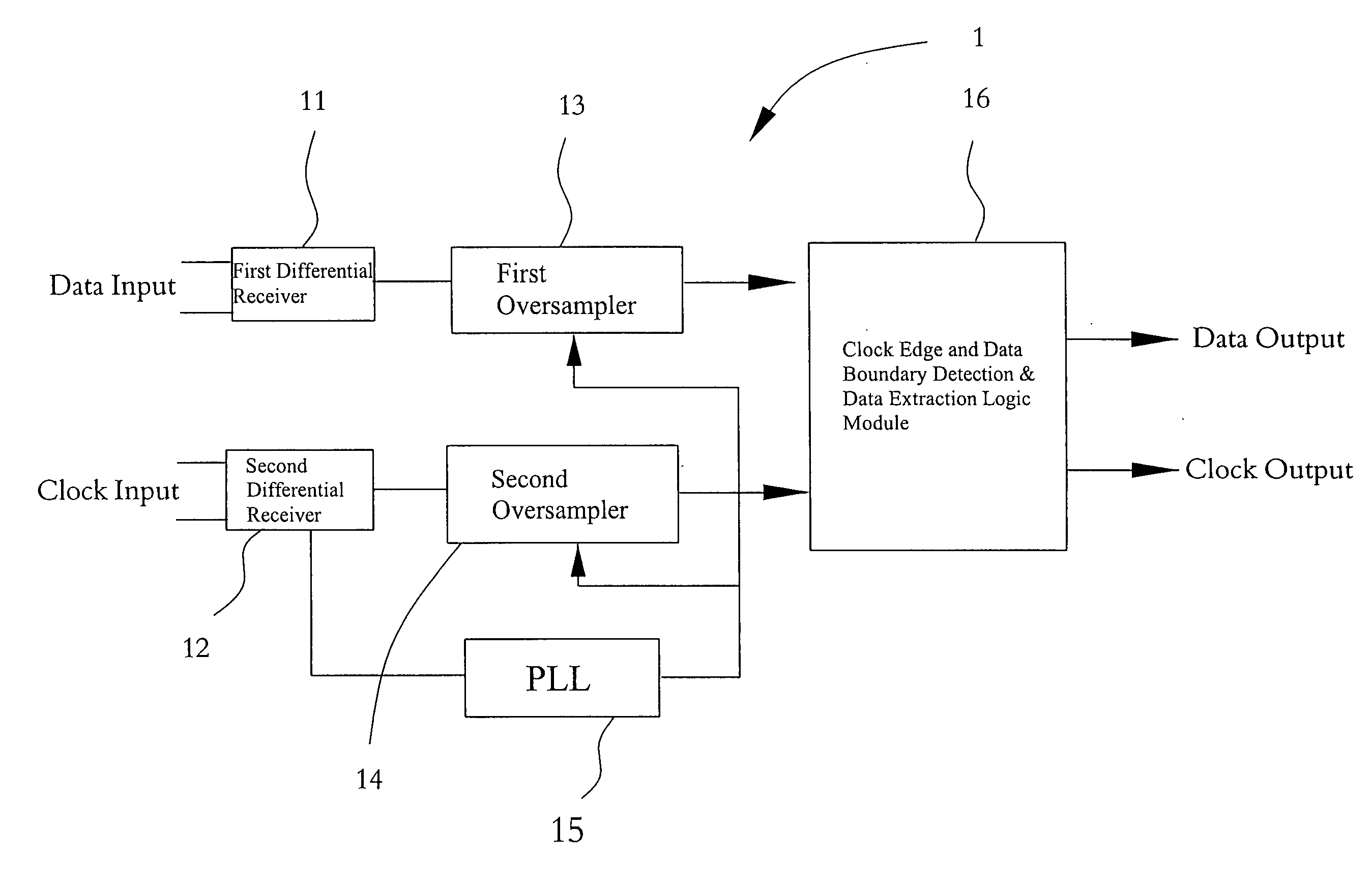
[0021]Please refer to FIG. 3 that is an implementation framework diagram of a low voltage differential signal receiving device 1 according to the present invention. As shown, the low voltage differential signal receiving (LVDS) device 1 includes a first differential receiver 11, a second differential receiver 12, a phase locked loop (PLL) 15, and a clock edge and data boundary detection and data extraction logic module 16.

[0022]The first differential receiver 11 receives a data signal from a data signal input, and sequentially outputs the received data signal to a first oversampler 13 and the clock edge and data boundary detection and data extraction logic module 16. When there is more than one data signal input, the first differential receiver 11 and the first oversampler 13 may be in a number corresponding to that of the data signal input to receive multiple data signals at the same time.

[0023]The second differential receiver 12 receives a clock signal and sequentially outputs the...


PUM


Abstract

A low voltage differential signal receiving device includes two differential receivers, two oversamplers, a phase locked loop, and a clock edge and data boundary detection & data extraction logic module. Clock and data signals are transmitted via channels having the same circuit layout, so that the clock signal is treated as another type of data signal. A frequency of sampling input clock and data is increased via asynchronous clock, clock transition is detected, and data bytes are extracted from clock and data samples. Therefore, the clock signal and the data signal have the same delay time to avoid any sampling error due to a difference in time sequence between the clock and the data. Meanwhile, due to the accurately increased sampling frequency, the sampled clock and the data signals are not adversely affected by different factors to enable upgraded data transmission efficiency and quality at the same time.

Description

FIELD OF THE INVENTION[0001]The present invention relates to a low voltage differential signal receiving device, and more particularly to a low voltage differential signal receiving device capable of upgrading the transmission quality and efficiency of low voltage differential signals.BACKGROUND OF THE INVENTION[0002]Processors being developed in recent years have a largely increased operation speed, and the quantity of data being processed within unit time is constantly increased. Thus, either the transmission of data between a computer and peripheral equipment, or various applications of integrated circuit (IC) products must rely on an interface circuit capable of transmitting and receiving very large amount of data. While an optical fiber may be used to transmit data over a long distance from a few decades to a few hundreds of kilometers, it is impractical to use the optical fiber to transmit data within a few meters or between different on-chip buses on a circuit board. Therefor...

Claims


Application Information

Patent Timeline
IPC IPC(8): G06F3/038
CPCG06F1/10
Inventor CHEN, YUNG-JANNLIEN, CHIU-FENG
Owner EXPLORE SEMICON
Why Eureka
Try Eureka