This helps you quickly interpret patents by identifying the three key elements:
Problems solved by technology
Method used
Benefits of technology
Benefits of technology
[0011]In a display device in this specification, a gate electrode of a transistor, which is connected to a gate electrode of a bootstrap transistor, is provided with a switch controlled by a start signal. When the start signal is input, a potential is supplied to the gate electrode of the transistor through the switch, and the transistor is turned off. The transistor is turned off, so that leakage of a charge from the gate electrode of the bootstrap transistor can be prevented. Accordingly, time for storing a charge in the gate electrode of the bootstrap transistor can be shortened, and high-speed operation can be performed.
[0069]With a structure disclosed in this specification, a shift register can operate with high speed. In particular, even when amorphous silicon is used as a semiconductor layer of a transistor, a shift register can operate with high speed. Therefore, a semiconductor device such as a liquid crystal display device, to which the shift register is applied, can operate with high speed, and increase in size or high definition of the semiconductor device can be easily realized.
Problems solved by technology
However, in the related art, time is required to make the gate electrode of the bootstrap transistor in a floating state while the bootstrap transistor is kept on; therefore, there is a problem that high-speed operation cannot be performed.
That is, a circuit technique for operating a shift register with high speed and a circuit technique for suppressing variation of a threshold voltage of a transistor remain as problems which cannot be solved by the related art.
Further, a technique for reducing the number of connection points of a driver IC mounted on a display panel, reduction in power consumption of a display device, and increase in size or definition of a display device also remain as problems.
Method used
Image
Click on the blue label to locate the original text in one second.
Reading with bidirectional positioning of images and text.
Examples
embodiment mode 1
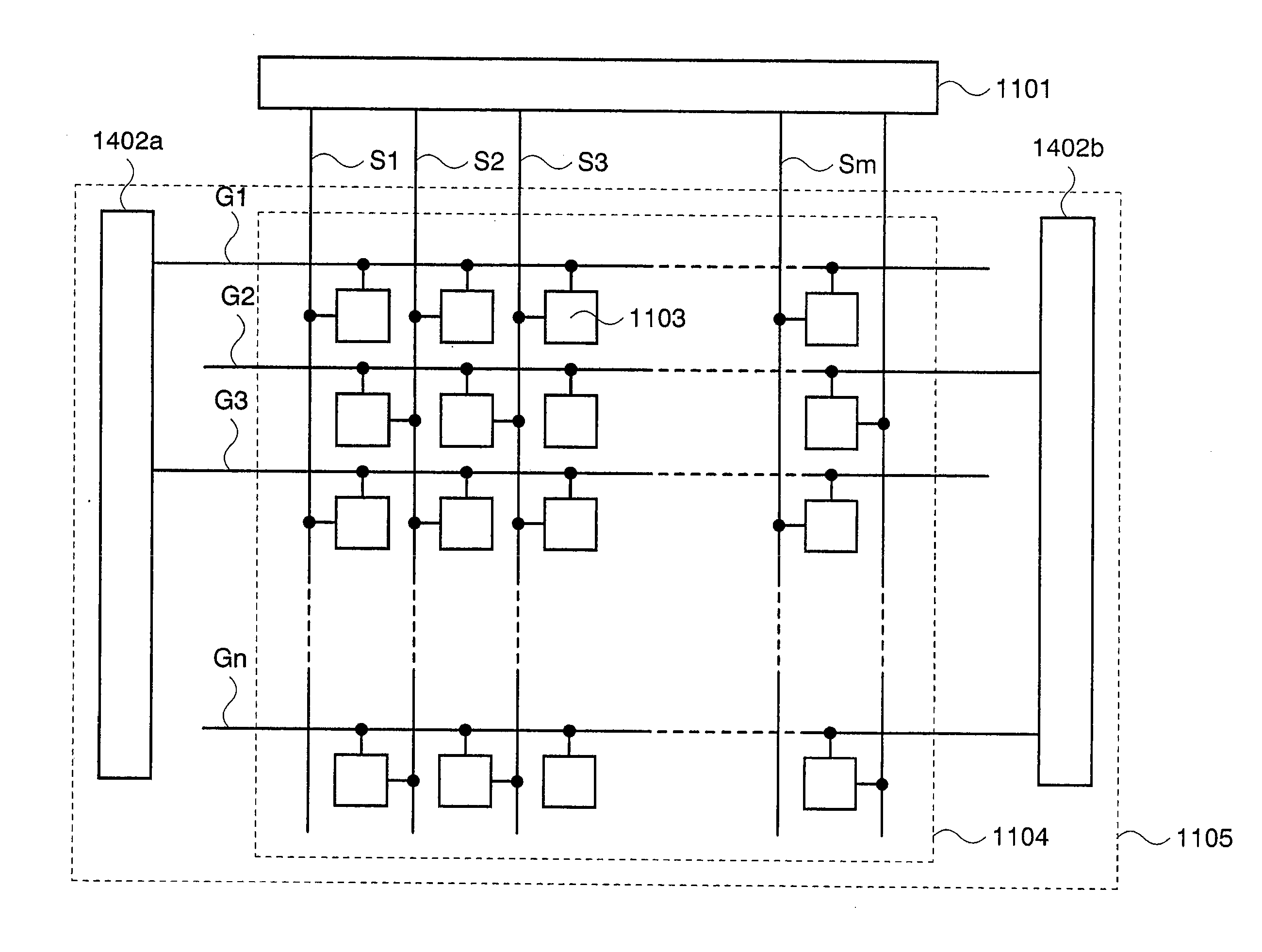
[0171]In this embodiment mode, structures and driving methods of a flip-flop, a driver circuit including the flip-flop, and a display device including the driver circuit are described.
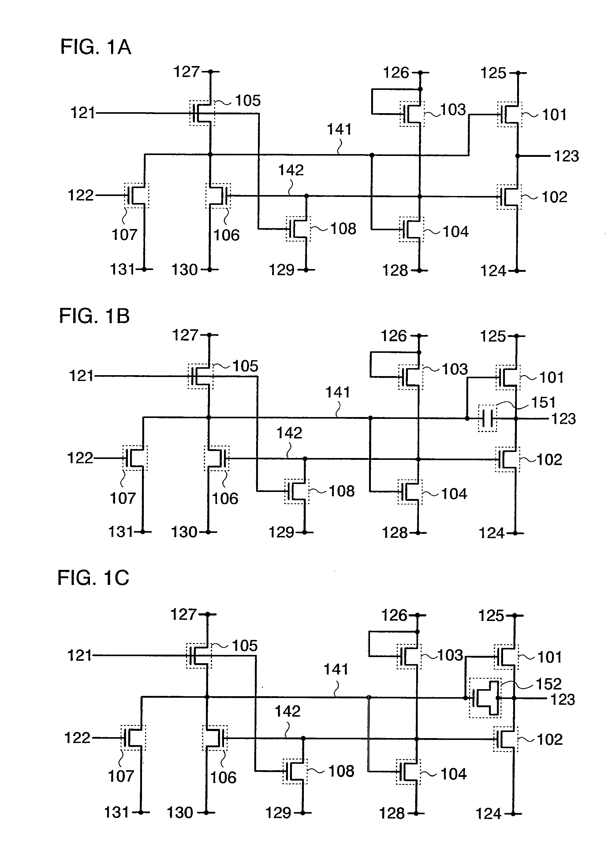
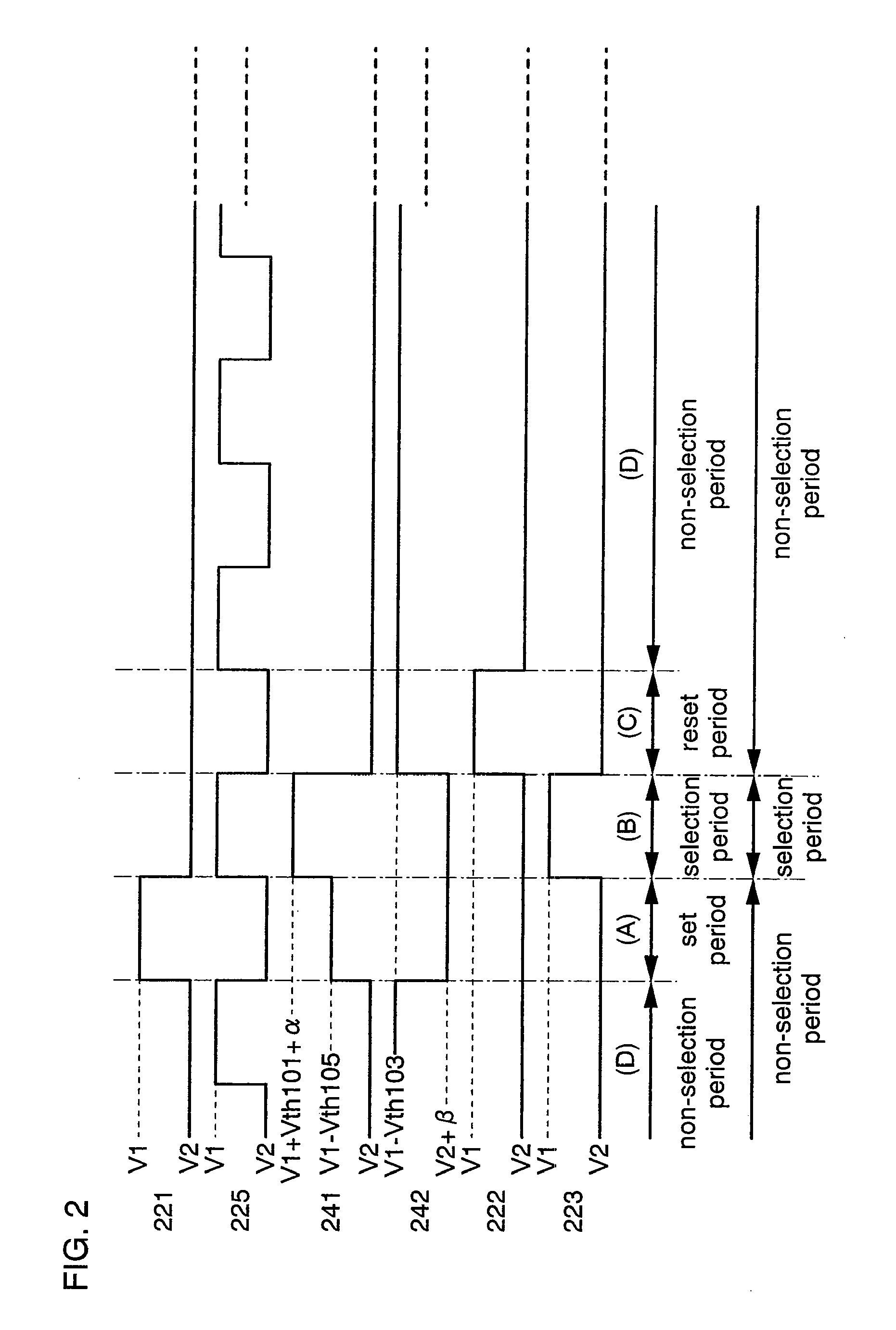
[0172]A basic structure of a flip-flop in this embodiment mode is described with reference to FIG. 1A. A flip-flop of FIG. 1A includes a first transistor 101, a second transistor 102, a third transistor 103, a fourth transistor 104, a fifth transistor 105, a sixth transistor 106, a seventh transistor 107, and an eighth transistor 108. In this embodiment mode, the first transistor 101, the second transistor 102, the third transistor 103, the fourth transistor 104, the fifth transistor 105, the sixth transistor 106, the seventh transistor 107, and the eighth transistor 108 are n-channel transistors and each of them is turned on when a gate-source voltage (Vgs) exceeds a threshold voltage (Vth).
[0173]In the flip-flop in this embodiment mode, all the first to eighth transistors 101 to 108 are n-channel tra...
embodiment mode 2
[0260]In this embodiment mode, structures and driving methods of a flip-flop different from those in Embodiment Mode 1, a driver circuit including the flip-flop, and a display device including the driver circuit are described. Note that portions common to Embodiment Mode 1 are denoted by common reference numerals, and detailed description of the same portions and portions having similar functions is omitted.
[0261]As a structure of a flip-flop in this embodiment mode, a structure similar to that of the flip-flop in Embodiment Mode 1 can be used. Thus, in this embodiment mode, description of the structure of the flip-flop is omitted. Note that timing for driving the flip-flop is different from that in Embodiment Mode 1.
[0262]The case where driving timing in this embodiment mode is applied to FIG. 1A is described. Note that the driving timing in this embodiment mode can be freely combined with each flip-flop in FIGS. 1B, 1C, 4A to 4C, 5A, and 5B as well. Further, the driving timing in ...
embodiment mode 3
[0290]In this embodiment mode, structures and driving methods of a flip-flop different from those in Embodiment Modes 1 and 2, a driver circuit including the flip-flop, and a display device including the driver circuit are described. In a flip-flop in this embodiment mode, an output signal and a transfer signal of the flip-flop are output from different wirings by different transistors. Note that portions common to Embodiment Modes 1 and 2 are denoted by common reference numerals, and detailed description of the same portions and portions having similar functions is omitted.
[0291]A basic structure of a flip-flop in this embodiment mode is described with reference to FIG. 23. The flip-flop in FIG. 23 is similar to the flip-flop in FIG. 1A to which a ninth transistor 109 and a tenth transistor 110 are added.
[0292]Connection relationships of the flip-flop in FIG. 23 are described. A first electrode of the ninth transistor 109 is connected to a thirteenth wiring 133, a second electrode ...
PUM
Abstract
An object of the invention is to provide a circuit technique which enables reduction in power consumption and high definition of a display device. A switch controlled by a start signal is provided to a gate electrode of a transistor, which is connected to a gate electrode of a bootstrap transistor. When the start signal is input, a potential is supplied to the gate electrode of the transistor through the switch, and the transistor is turned off. The transistor is turned off, so that leakage of a charge from the gate electrode of the bootstrap transistor can be prevented. Accordingly, time for storing a charge in the gate electrode of the bootstrap transistor can be shortened, and high-speed operation can be performed.
Description
BACKGROUND OF THE INVENTION[0001]1. Field of the Invention[0002]The present invention relates to a display device including a circuit formed using a transistor. In particular, the present invention relates to a display device using an electrooptical element such as a liquid crystal element, a light-emitting element, or the like, and an operation method thereof.[0003]2. Description of the Related Art[0004]In recent years, with the increase of large display devices such as liquid crystal televisions, display devices have been actively developed. In particular, a technique for forming a pixel circuit and a driver circuit including a shift register and the like (hereinafter also referred to as an internal circuit) over the same insulating substrate by using transistors formed of a non-crystalline semiconductor (hereinafter also referred to as amorphous silicon) has been actively developed because the technique greatly contributes to reduction in power consumption and cost. The internal ...
Claims
Application Information
Patent Timeline
Application Date:The date an application was filed.
Publication Date:The date a patent or application was officially published.
First Publication Date:The earliest publication date of a patent with the same application number.
Issue Date:Publication date of the patent grant document.
PCT Entry Date:The Entry date of PCT National Phase.
Estimated Expiry Date:The statutory expiry date of a patent right according to the Patent Law, and it is the longest term of protection that the patent right can achieve without the termination of the patent right due to other reasons(Term extension factor has been taken into account ).
Invalid Date:Actual expiry date is based on effective date or publication date of legal transaction data of invalid patent.

