Stressed field effect transistor and methods for its fabrication

a field effect transistor and stress-sensitive technology, applied in the direction of basic electric elements, electrical apparatus, semiconductor devices, etc., can solve the problems that no one has yet achieved the mobility potential attainable with embedded silicon germanium, and achieve the effect of enhancing the mobility of the majority carrier

Active Publication Date: 2008-04-03
TAIWAN SEMICON MFG CO LTD
View PDF12 Cites 38 Cited by
  • Summary
  • Abstract
  • Description
  • Claims
  • Application Information

AI Technical Summary

Benefits of technology

[0005]A stressed field effect transistor having enhanced majority carrier mobility is provided. The stressed field effect transistor comprises a silicon substrate with a gate insulator overlying the silicon substrate. A gate electrode overlies the gate insulator and defines a channel region in the silicon substrate underlying the gate electrode. A first silicon germanium region having a first thickness is embedded in the silicon substrate and contacts the channel region. A second silicon germanium region having a second thickness greater than the first thickness and spaced apart from the channel region is also embedded in the silicon substrate.
[0006]Methods are provided for fabricating a stressed field effect transistor having enhanced majority carrier mobility. The method comprises forming a silicon on insulator substrate comprising a layer of silicon on a layer of insulator on a silicon substrate. A gate electrode is formed overlying the layer of silicon. A first undoped silicon germanium layer is epitaxially embedded into the silicon layer and aligned with the gate electrode. A second impurity doped silicon germanium layer is epitaxially embedded into the silicon layer and spaced apart from the gate electrode.

Problems solved by technology

Although a number of techniques are know for embedding SiGe to enhance the mobility of majority carrier holes in PFETs, none has yet achieved the increase in mobility potentially attainable with embedded silicon germanium.

Method used


Image

  • Stressed field effect transistor and methods for its fabrication
  • Stressed field effect transistor and methods for its fabrication
  • Stressed field effect transistor and methods for its fabrication

Examples


Embodiment Construction

[0012]The following detailed description is merely exemplary in nature and is not intended to limit the invention or the application and uses of the invention. Furthermore, there is no intention to be bound by any expressed or implied theory presented in the preceding technical field, background, brief summary or the following detailed description.

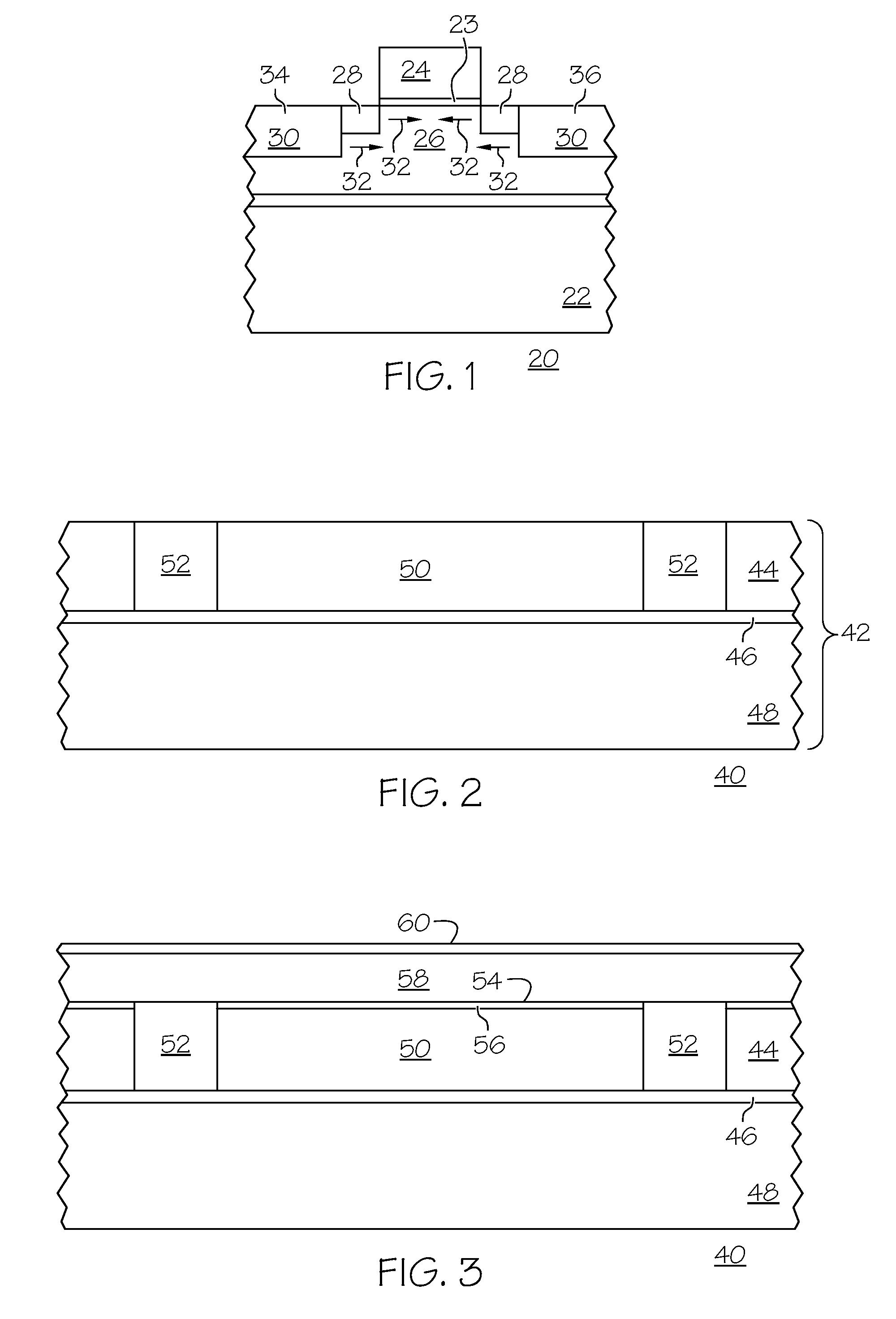
[0013]FIG. 1 schematically illustrates, in cross section, a field effect transistor (FET) 20, specifically a P-channel FET (PFET), in accordance with one embodiment of the invention. FET 20 includes a silicon substrate 22 having a gate insulator 23 formed at the substrate surface. A gate electrode 24 overlies the gate insulator. The gate electrode defines the location of a transistor channel 26 at the substrate surface and underlying the gate electrode. A shallow region of preferably undoped silicon germanium (SiGe) 28 is embedded into the silicon substrate in close proximity to the edges of the transistor channel. A deeper region of prefe...


PUM


Abstract

A stressed field effect transistor and methods for its fabrication are provided. The field effect transistor comprises a silicon substrate with a gate insulator overlying the silicon substrate. A gate electrode overlies the gate insulator and defines a channel region in the silicon substrate underlying the gate electrode. A first silicon germanium region having a first thickness is embedded in the silicon substrate and contacts the channel region. A second silicon germanium region having a second thickness greater than the first thickness and spaced apart from the channel region is also embedded in the silicon substrate.

Description

TECHNICAL FIELD[0001]The present invention generally relates to stressed field effect transistors and to methods for their fabrication, and more particularly relates to embedded silicon germanium stressed field effect transistors and to methods for their fabrication.BACKGROUND[0002]The majority of present day integrated circuits (ICs) are implemented by using a plurality of interconnected field effect transistors (FETs), also called metal oxide semiconductor field effect transistors (MOSFETs), or simply MOS transistors. A FET includes a gate electrode as a control electrode and spaced apart source and drain electrodes between which a current can flow. A control voltage applied to the gate electrode controls the flow of current through a channel between the source and drain electrodes.[0003]The gain of an FET, usually defined by the transconductance (gm), is proportional to the mobility of the majority carrier in the transistor channel. The current carrying capability of an MOS trans...

Claims


Application Information

Patent Timeline
Patent Type & Authority Applications(United States)
IPC IPC(8): H01L29/78H01L21/336
CPCH01L21/823807H01L21/823814H01L29/7848H01L29/6656H01L29/66636H01L29/6653H01L29/772H01L21/18
Inventor WAITE, ANDREW M.LUNING, SCOTT
Owner TAIWAN SEMICON MFG CO LTD
Why Eureka
Try Eureka